The DM816x DaVinci video processors are a highly integrated, programmable platform that leverages TI"s DaVinci technology to meet the processing needs of the following applications: video encode, decode, transcode, and transrate; video security; video conferencing; video infrastructure; media server; and digital signage.
The device enables original-equipment manufacturers (OEMs) and original-design manufacturers (ODMs) to quickly bring to market devices featuring robust operating systems support, rich user interfaces, and high processing performance through the maximum flexibility of a fully integrated mixed processor solution. The device combines programmable video and audio processing with a highly integrated peripheral set.
Key to the device are up to three high-definition video and imaging coprocessors (HDVICP2). Each coprocessor can perform a single 1080p60 H.264 encode or decode or multiple lower resolution or frame rate encodes and decodes. Multichannel HD-to-HD or HD-to-SD transcoding and multicoding are also possible. With the ability to simultaneously process 1080p60 streams, the TMS320DM816x device is a powerful solution for today"s demanding HD video application requirements.
Programmability is provided by an ARM Cortex-A8 RISC CPU with NEON extension, TI C674x VLIW floating-point DSP core, and high-definition video and imaging coprocessors. The ARM processor lets developers keep control functions separate from audio and video algorithms programmed on the DSP and coprocessors, thus reducing the complexity of the system software. The ARM Cortex-A8 32-bit RISC processor with NEON floating-point extension includes: 32KB of instruction cache; 32KB of data cache; 256KB of L2 cache; 48KB of public ROM, and 64KB of RAM.
The rich peripheral set provides the ability to control external peripheral devices and communicate with external processors. For details on each peripheral, see the related sections in this document and the associated peripheral reference guides. The peripheral set includes: HD video processing subsystem (HDVPSS), which provides output of simultaneous HD and SD analog video and dual HD video inputs; up to two Gigabit Ethernet MACs (10 Mbps,100, Mbps, 1000 Mbps) with GMII and MDIO interface; two USB ports with integrated 2.0 PHY; PCIe port x2 lanes GEN2 compliant interface, which allows the device to act as a PCIe root complex or device endpoint; one 6-channel McASP audio serial port (with DIT mode); two dual-channel McASP audio serial ports (with DIT mode); one McBSP multichannel buffered serial port; three UARTs with IrDA and CIR support; SPI serial interface; SD and SDIO serial interface; two I2C master and slave interfaces; up to 64 GPIO pins; seven 32-bit timers; system watchdog timer; dual DDR2 and DDR3 SDRAM interface; flexible 8-bit and 16-bit asynchronous memory interface; and up to two SATA interfaces for external storage on two disk drives or more with the use of a port multiplier.
The device also includes an SGX530 3D graphics engine (available only on the TMS320DM8168 device) to enable sophisticated GUIs and compelling user interfaces and interactions. Additionally, the device has a complete set of development tools for both the ARM and DSP, including C compilers, a DSP assembly optimizer to simplify programming and scheduling, and a Microsoft Windows debugger interface for visibility into source code execution.
The C674x DSP core is the high-performance floating-point DSP generation in the TMS320C6000 DSP platform. The C674x floating-point DSP processor uses 32KB of L1 program memory and 32KB of L1 data memory. Up to 32KB of L1P can be configured as program cache. The remaining is noncacheable no-wait-state program memory. Up to 32KB of L1D can be configured as data cache. The remaining is noncacheable no-wait-state data memory. The DSP has 256KB of L2 RAM, which can be defined as SRAM, L2 cache, or a combination of both. All C674x L3 and off-chip memory accesses are routed through a system MMU.
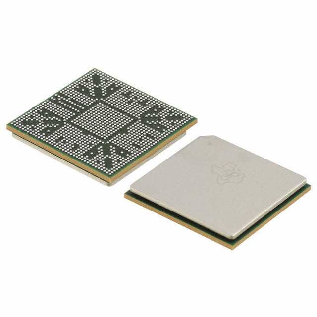
The device package has been specially engineered with Via Channel technology. This technology allows use of 0.8-mm pitch PCB feature sizes in this 0.65-mm pitch package, and substantially reduces PCB costs. Via Channel technology also allows PCB routing in only two signal layers due to the increased layer efficiency of the Via Channel BGA technology.