
下载

DS190 (v1.9) January 20, 2016 www.xilinx.com
Product Specification 1
© Copyright 2012–2016 Xilinx, Inc., Xilinx, the Xilinx logo, Artix, ISE, Kintex, Spartan, Virtex, Vivado, Zynq, and other designated brands included herein are trademarks of Xilinx
in the United States and other countries. AMBA, AMBA Designer, ARM, ARM Cortex-A9, CoreSight, Cortex, and PrimeCell are trademarks of ARM in the EU and other countries.
PCI, PCIe, and PCI Express are trademarks of PCI-SIG and used under license. All other trademarks are the property of their respective owners.
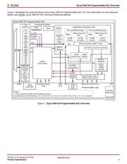
Zynq-7000 All Programmable SoC First Generation Architecture
The Zynq®-7000 family is based on the Xilinx All Programmable SoC architecture. These products integrate a feature-rich dual-core
ARM® Cortex™-A9 based processing system (PS) and 28 nm Xilinx programmable logic (PL) in a single device. The ARM Cortex-A9
CPUs are the heart of the PS and also include on-chip memory, external memory interfaces, and a rich set of peripheral connectivity
interfaces.
Processing System (PS)
Dual-core ARM® Cortex™-A9 Based
Application Processor Unit (APU)
• 2.5 DMIPS/MHz per CPU
• CPU frequency: Up to 1 GHz
• Coherent multiprocessor support
• ARMv7-A architecture
• TrustZone® security
• Thumb®-2 instruction set
• Jazelle® RCT execution Environment Architecture
• NEON™ media-processing engine
• Single and double precision Vector Floating Point Unit (VFPU)
• CoreSight™ and Program Trace Macrocell (PTM)
• Timer and Interrupts
• Three watchdog timers
• One global timer
• Two triple-timer counters
Caches
• 32 KB Level 1 4-way set-associative instruction and data caches
(independent for each CPU)
• 512 KB 8-way set-associative Level 2 cache
(shared between the CPUs)
• Byte-parity support
On-Chip Memory
• On-chip boot ROM
• 256 KB on-chip RAM (OCM)
• Byte-parity support
External Memory Interfaces
• Multiprotocol dynamic memory controller
• 16-bit or 32-bit interfaces to DDR3, DDR3L, DDR2, or LPDDR2
memories
• ECC support in 16-bit mode
• 1GB of address space using single rank of 8-, 16-, or 32-bit-wide
memories
• Static memory interfaces
• 8-bit SRAM data bus with up to 64 MB support
• Parallel NOR flash support
• ONFI1.0 NAND flash support (1-bit ECC)
• 1-bit SPI, 2-bit SPI, 4-bit SPI (quad-SPI), or two quad-SPI (8-bit)
serial NOR flash
8-Channel DMA Controller
• Memory-to-memory, memory-to-peripheral, peripheral-to-memory,
and scatter-gather transaction support
I/O Peripherals and Interfaces
• Two 10/100/1000 tri-speed Ethernet MAC peripherals with
IEEE Std 802.3 and IEEE Std 1588 revision 2.0 support
• Scatter-gather DMA capability
• Recognition of 1588 rev. 2 PTP frames
• GMII, RGMII, and SGMII interfaces
• Two USB 2.0 OTG peripherals, each supporting up to 12 Endpoints
• USB 2.0 compliant device IP core
• Supports on-the-go, high-speed, full-speed, and low-speed
modes
• Intel EHCI compliant USB host
• 8-bit ULPI external PHY interface
• Two full CAN 2.0B compliant CAN bus interfaces
• CAN 2.0-A and CAN 2.0-B and ISO 118981-1 standard
compliant
• External PHY interface
• Two SD/SDIO 2.0/MMC3.31 compliant controllers
• Two full-duplex SPI ports with three peripheral chip selects
• Two high-speed UARTs (up to 1 Mb/s)
• Two master and slave I2C interfaces
• GPIO with four 32-bit banks, of which up to 54 bits can be used with
the PS I/O (one bank of 32b and one bank of 22b) and up to 64 bits
(up to two banks of 32b) connected to the Programmable Logic
• Up to 54 flexible multiplexed I/O (MIO) for peripheral pin assignments
Interconnect
• High-bandwidth connectivity within PS and between PS and PL
• ARM AMBA® AXI based
• QoS support on critical masters for latency and bandwidth control
Programmable Logic (PL)
Configurable Logic Blocks (CLB)
• Look-up tables (LUT)
• Flip-flops
• Cascadeable adders
36 Kb Block RAM
• True Dual-Port
• Up to 72 bits wide
• Configurable as dual 18 Kb block RAM
DSP Blocks
• 18 x 25 signed multiply
• 48-bit adder/accumulator
• 25-bit pre-adder
Zynq-7000 All Programmable SoC Overview
DS190 (v1.9) January 20, 2016 Product Specification