

下载
DS073 (v2.0) April 7, 2014 www.xilinx.com
Product Specification 1
© Copyright 2000–2014 Xilinx, Inc. XILINX, the Xilinx logo, Virtex, Spartan, ISE, and other designated brands included herein are trademarks of Xilinx in the United States and
other countries. All other trademarks are the property of their respective owners.
— OBSOLETE — OBSOLETE — OBSOLETE — OBSOLETE — OBSOLETE —
Features
• One-time programmable (OTP) read-only memory
designed to store configuration bitstreams of
Xilinx® FPGA devices
• Simple interface to the FPGA
• Cascadable for storing longer or multiple bitstreams
• Programmable reset polarity (active High or active
Low) for compatibility with different FPGA solutions
• Low-power CMOS floating-gate process
• 3.3V supply voltage
• Guaranteed 20 year life data retention
• Available in compact plastic packages: VQ44, PC44,
PC20, VO8, and SO20
(1)
• Programming support by leading programmer
manufacturers
• Design support using the ISE® Foundation™ and
ISE WebPACK™ software
• Dual configuration modes for the XC17V16 and
XC17V08
(1)
devices
♦ Serial slow/fast configuration (up to 20 Mb/s)
♦ Parallel (up to 160 Mb/s at 20 MHz)
Description
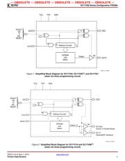
Xilinx introduces the high-density XC17V00 family of
configuration PROMs which provide an easy-to-use, cost-
effective method for storing large Xilinx FPGA configuration
bitstreams. Initial devices in the 3.3V family are available in
16 Mb, 8 Mb, 4 Mb, 2 Mb, and 1 Mb densities. See Figure 1
and Figure 2 for simplified block diagrams of the XC17V00
family.
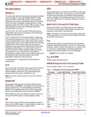
The XC17V00 PROM can configure a Xilinx FPGA using
the FPGA serial configuration mode interface. When the
FPGA is in Master Serial mode, it generates a configuration
clock that drives the PROM. A short access time after the
rising clock edge, data appears on the PROM DATA output
pin that is connected to the FPGA DIN pin. The FPGA
generates the appropriate number of clock pulses to
complete the configuration. Once configured, it disables the
PROM. When the FPGA is in Slave Serial mode, the PROM
and the FPGA must both be clocked by an incoming signal.
The XC17V08
(1)
and XC17V16 PROM can optionally
configure a Xilinx FPGA using the FPGA Parallel
(SelectMAP) configuration mode interface. When the FPGA
is in Master SelectMAP mode, the FPGA generates the
configuration clock that drives the PROM.
When the FPGA is in Slave SelectMAP mode, an external,
free-running oscillator generates the configuration clock
that drives the PROM and the FPGA. After the rising
configuration clock (CCLK) edge, data is available on the
PROMs DATA (D0-D7) pins. The data is clocked into the
FPGA on the following rising edge of the CCLK (Figure 3).
Multiple PROMs can be concatenated by using the CEO
output to drive the CE
input of the following device. The
clock inputs and the DATA outputs of all PROMs in this
chain are interconnected. All devices are compatible and
can be cascaded with other members of the family.
For device programming, either the Xilinx ISE Foundation or
ISE WebPACK software compiles the FPGA design file into
a standard Hex format, which is then transferred to most
commercial PROM programmers.
0
XC17V00 Series Configuration PROMs
DS073 (v2.0) April 7, 2014
08
Product Specification
R
1. Specific part number and package combinations have been discontinued. Refer to XCN07010. Discontinued part number and package combinations
remain in this data sheet for reference.