

下载
28 Gbps, 5-Bit, Digital Time Delay with
Programmable Output Voltage
Data Sheet
HMC856
Rev. C Document Feedback
Information furnished by Analog Devices is believed to be accurate and reliable. However, no
responsibility is assumed by Analog Devices for its use, nor for any infringements of patents or other
rights of third parties that may result from its use. Specifications subject to change without notice. No
license is granted by implication or otherwise under any patent or patent rights of Analog Devices.
Trademarks and registered trademarks are the property of their respective owners.
One Technology Way, P.O. Box 9106, Norwood, MA 02062-9106, U.S.A.
Tel: 781.329.4700 ©2016 Analog Devices, Inc. All rights reserved.
Technical Support www.analog.com
FEATURES
Differential and single-ended operation
Supports data rates up to 28 Gbps
Fast rise/fall time: 20 ps/18 ps
Low power consumption: 610 mW typical
Programmable differential
Output voltage swing: 500 mV p-p to 1350 mV p-p
Single supply: −3.3 V
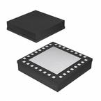
5 mm × 5 mm, 32-terminal ceramic leadless chip carrier (LCC)
package: 25 mm
2
APPLICATIONS
SONET OC-192
High speed serial logic
Clock and data recovery
Broadband test and measurement equipment
Frequency synthesis
Matched timing
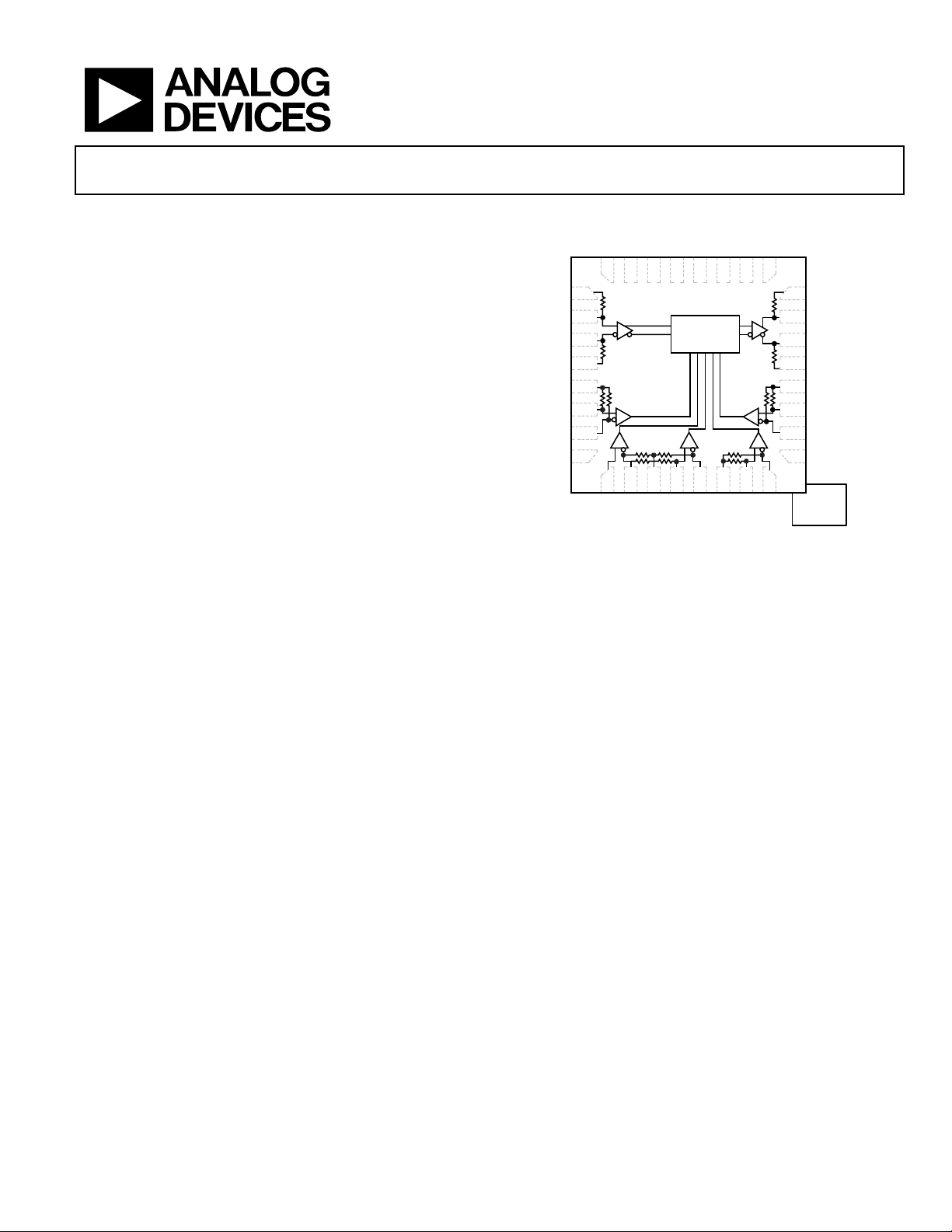
FUNCTIONAL BLOCK DIAGRAM
17
1
50Ω
50Ω
50Ω
50Ω
600Ω 600Ω
600Ω 600Ω
600Ω
3
4
2
9
GND
I+
I–
GND
5
6
GND
B0+
7B0–
8NC NC
18 B4–
19 B4+
20 GND
21 GND
22 O–
23 O+
24 GND
B1+
12
B2+
11
GND
10
B1–
13
B2–
14
GND
15
B3+
16
B3–
25
NIC
26
GND
27
V
EE
28
VR
29
VB
30
V
EE
31
GND
32
NIC
PACKAGE
BASE
V
EE
DELAY
HMC856
14720-001
F
igure 1.
GENERAL DESCRIPTION
The HMC856 is a wideband time delay device with a 5-bit
digital control designed for timing compensation or clock skew
management applications. The time delay provides nearly
100 ps (maximum) of delay range with 3 ps resolution and
supports 28 Gbps data. The monotonic delay is compensated
for stable operation over both power supply and temperature
variation.
All differential inputs to the HMC856 are current mode logic
(CML) and terminated on chip with 50 Ω to the positive supply
ground, GND, and can be ac or dc-coupled. The differential CML
outputs are source terminated to 50 Ω and can also be ac or dc-
coupled. Connect outputs directly to a 50 Ω ground terminated
system or drive devices with CML logic input. The control lines,
B4 to B0, are differential CML inputs terminated with 600 Ω to
the positive rail, which supports lower power control options.
The HMC856 features an output level control pin, VR, that
allows loss compensation or signal level optimization. The
HMC856 operates from a single −3.3 V supply and is available
in a 5 mm × 5 mm LCC package.
页面指南