

下载

For price, delivery and to place orders: Hittite Microwave Corporation, 2 Elizabeth Drive, Chelmsford, MA 01824
Phone: 978-250-3343 Fax: 978-250-3373 Order On-line at www.hittite.com
Application Support: Phone: 978-250-3343 or apps@hittite.com
FREQUENCY DIVIDERS & DETECTORS - SMT
1
HMC794LP3E
v01.0612
2 GHz LOW NOISE PROGRAMMABLE
DIVIDER (N = 1 to 4)
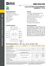
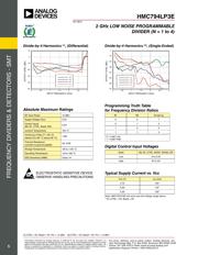
General Description
Features
Functional Diagram
Typical Applications
The HMC794LP3E is a SiGe BiCMOS low noise
programmable frequency divider in a 3x3mm lead-
less surface mount package. The circuit can be
programmed to divide from N = 1 to N = 4 in the
200 MHz to 2 GHz input frequency range. The high
level output power (up to 10 dBm) with a very low
SSB phase noise and 50% duty cycle makes this
device ideal for low noise clock generation, LO
generation and LO drive applications. Congurable
bias controls allow power minimization of up to 20%.
Low Noise Floor: -163 dBc/Hz at 10 MHz offset
and -160 dBc/Hz at 100 kHz offset
Programmable Frequency Divider, N = 1, 2, 3 or 4
200 MHz to 2 GHz Input Frequency Range
50% Duty Cycle Outputs
Up to +10 dBm Output Power
Sleep Mode: Consumes <1 µA
16 Lead 3X3 mm SMT Package: 9mm
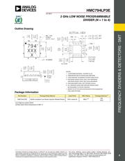
2
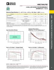
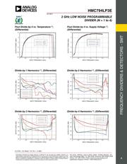
Electrical Specications, T
A
= +25° C, Vcc = +5V, Z
o
= 50Ω, Bias1 = GND
The HMC794LP3E is ideal for:
• LO Generation with Low Noise Floor
• Clock Generators
• Mixer LO Drive
• Military Applications
• Test Equipment
• Sensors
Parameter Conditions Min. Typ. Max. Units
RF Input Characteristics
Max RF Input Frequency 2 GHz
Min RF Input Frequency 200 MHz
RF Input Power Note: best SSB Phase Noise for Pin > 5 dBm -2 3 10 dBm
Divider Output Characteristics
Differential Output Power
Programmable in 2 steps
(see the Pout plots for each division ratio)
-3 10 12 dBm
SSB Phase Noise @ 10 MHz Offset
+5 dBm Input Power, 2 GHz Input
-163 dBc/Hz
SSB Phase Noise @ 100 kHz Offset -160 dBc/Hz
SSB Phase Noise @ 10 kHz Offset -153 dBc/Hz
Duty Cycle for Differential Mode +5 dBm Input Power 50 ±3 %
Logic Inputs
VIH Input High Voltage 3 5 V
VIL Input Low Voltage 0 0.4 V
Information furnished by Analog Devices is believed to be accurate and reliable. However, no
responsibility is assumed by Analog Devices for its use, nor for any infringements of patents or other
rights of third parties that may result from its use. Specifications subject to change without notice. No
license is granted by implication or otherwise under any patent or patent rights of Analog Devices.
Trademarks and registered trademarks are the property of their respective owners.
For price, delivery, and to place orders: Analog Devices, Inc.,
One Technology Way, P.O. Box 9106, Norwood, MA 02062-9106
Phone: 781-329-4700 • Order online at www.analog.com
Application Support: Phone: 1-800-ANALOG-D
页面指南