
下载
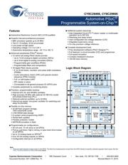
CY8C29466, CY8C29666
Automotive PSoC
®
Programmable System-on-Chip™
Cypress Semiconductor Corporation • 198 Champion Court • San Jose, CA 95134-1709 • 408-943-2600
Document Number: 001-12899 Rev. *H Revised March 17, 2015
Features
■ Automotive Electronics Council (AEC) Q100 qualified
■ Powerful Harvard-architecture processor
❐ M8C processor speeds up to 24 MHz
❐ Two 8 × 8 multiply, 32-bit accumulate
❐ Low power at high speed
❐ Operating voltage: 3.0 V to 5.25 V
❐ Automotive temperature range: –40 °C to +85 °C
■ Advanced peripherals (PSoC
®
blocks)
❐ 12 rail-to-rail analog PSoC blocks provide:
• Up to 14-bit analog-to-digital converters (ADCs)
• Up to 9-bit digital-to-analog converters (DACs)
• Programmable gain amplifiers (PGAs)
• Programmable filters and comparators
❐ 16 digital PSoC blocks provide:
• 8- to 32-bit timers, counters, and pulse width modulators
(PWMs)
• Cyclic redundancy check (CRC) and pseudo-random
sequence (PRS) modules
• Full- or half-duplex UART
• SPI master or slave
• Connectable to all general purpose I/O (GPIO) pins
❐ Complex peripherals by combining blocks
■ Precision, programmable clocking
❐ Internal ±5% 24- and 48-MHz oscillator
❐ High accuracy 24 MHz with optional 32.768 kHz crystal
and phase-locked loop (PLL)
❐ Optional external oscillator, up to 24 MHz
❐ Internal low-speed, low-power oscillator for watchdog and
sleep functionality
■ Flexible on-chip memory
❐ 32 KB flash program storage,
1000 erase/write cycles
❐ 2 KB SRAM data storage
❐ In-system serial programming (ISSP)
❐ Partial flash updates
❐ Flexible protection modes
❐ EEPROM emulation in flash
■ Programmable pin configurations
❐ 25 mA sink, 10 mA drive on all GPIOs
❐ Pull-up, pull-down, high Z, strong, or open drain drive modes
on all GPIOs
❐ Up to 12 analog inputs on GPIOs
[1]
❐ Four 30 mA analog outputs on GPIOs
❐ Configurable interrupt on all GPIOs
■ Additional system resources
❐ Inter-Integrated Circuit (I
2
C™) slave, master, or multimaster
operation up to 400 kHz
❐ Watchdog and sleep timers
❐ User-configurable low-voltage detection (LVD)
❐ Integrated supervisory circuit
❐ On-chip precision voltage reference
■ Complete development tools
❐ Free development software (PSoC Designer™)
❐ Full featured, in-circuit emulator (ICE) and programmer
❐ Full-speed emulation
❐ Complex breakpoint structure
❐ 128 KB trace memory
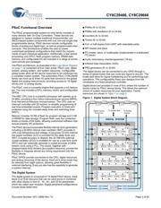
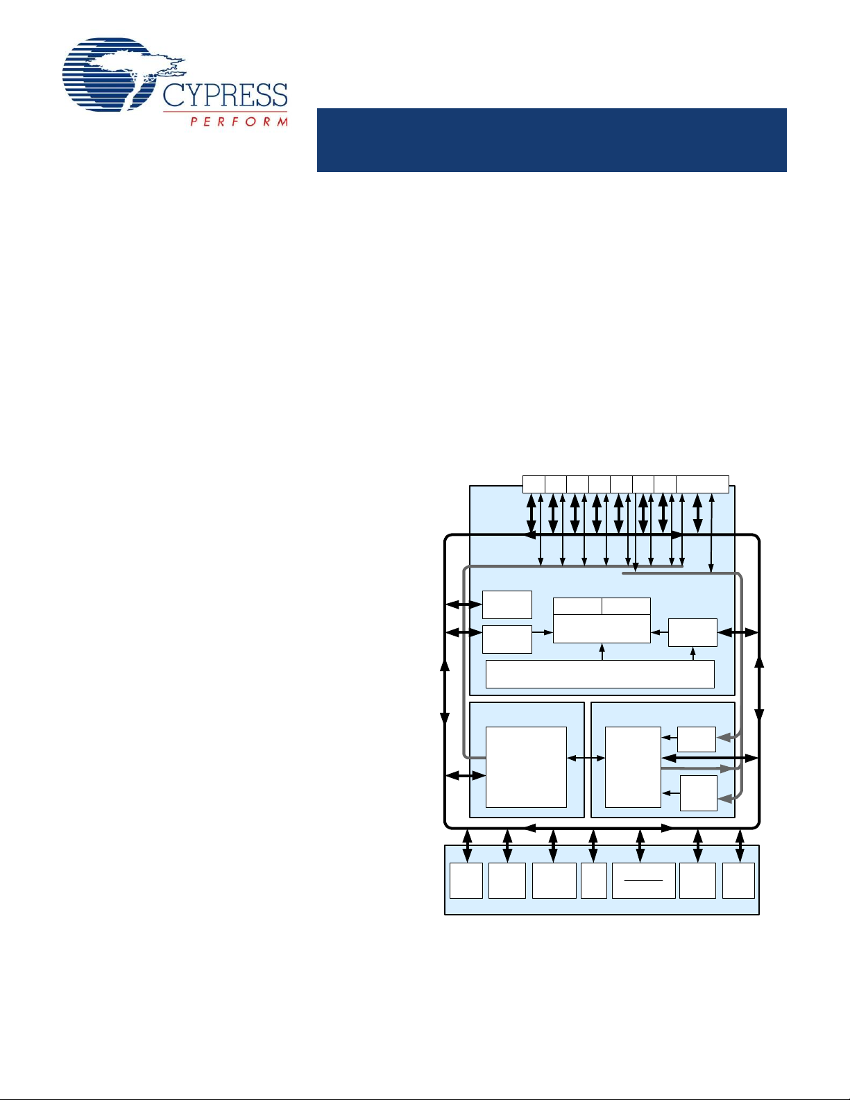
DIGITAL SYSTEM
SRAM
256 Bytes
Interrupt
Controller
Sleep and
Watchdog
Multiple Clock Sources
(Includes IMO, ILO, PLL, and ECO)
Global Digital Interconnect
Global Analog Interconnect
PSoC
CORE
CPU Core (M8C)
SROM Flash 16 KB
Digital
Block
Array
Multiply
Accum.
Switch
Mode
Pump
Internal
Voltage
Ref.
Digital
Clocks
POR and LVD
System Resets
Decimator
SYSTEM RESOURCES
ANALOG SYSTEM
Analog
Ref.
Analog
Input
Muxing
I
2
C
System Bus
Analog
Block
Array
Port
6
Port 0 with
Analog Drivers
Port
1
Port
2
Port
3
Port
4
Port
5
Port
7
Logic Block Diagram
Note
1. There are eight standard analog inputs on the GPIO. The other four analog inputs connect from the GPIO directly to specific switched-capacitor block inputs. See the
PSoC Technical Reference Manual for more details
页面指南