

下载
CY8C24094/CY8C24794
CY8C24894/CY8C24994
PSoC
®
Programmable System-on-Chip™
Cypress Semiconductor Corporation • 198 Champion Court • San Jose, CA 95134-1709 • 408-943-2600
Document Number: 38-12018 Rev. AK Revised March 12, 2015
PSoC
®
Programmable System-on-Chip
1. Features
■ XRES pin to support in-system serial programming (ISSP) and
external reset control in CY8C24894
■ Powerful Harvard-architecture processor
❐ M8C processor speeds up to 24 MHz
❐ Two 8 × 8 multiply, 32-bit accumulate
❐ Low power at high speed
❐ Operating voltage: 3 V to 5.25 V
❐ Industrial temperature range: –40 °C to +85 °C
❐ USB temperature range: –10 °C to +85 °C
■ Advanced peripherals (PSoC
®
Blocks)
❐ Six rail-to-rail analog PSoC blocks provide:
• Up to 14-bit analog-to-digital converters (ADCs)
• Up to 9-bit digital-to-analog converters (DACs)
• Programmable gain amplifiers (PGAs)
• Programmable filters and comparators
❐ Four digital PSoC blocks provide:
• 8- to 32-bit timers, counters, and pulse width modulators
(PWMs)
• Cyclical redundancy check (CRC) and pseudo random
sequence (PRS) modules
• Full-duplex universal asynchronous receiver transmitter
(UART)
• Multiple serial peripheral interface (SPI) masters or slaves
• Connectable to all general-purpose I/O (GPIO) pins
❐ Complex peripherals by combining blocks
❐ Capacitive sensing application (CSA) capability
■ Full speed USB (12 Mbps)
❐ Four unidirectional endpoints
❐ One bidirectional control endpoint
❐ USB 2.0 compliant
❐ Dedicated 256 byte buffer
❐ No external crystal required
■ Flexible on-chip memory
❐ 16 KB flash program storage 50,000 erase and write cycles
❐ 1 KB static random access memory (SRAM) data storage
❐ ISSP
❐ Partial flash updates
❐ Flexible protection modes
❐ Electrically erasable programmable read-only memory
(EEPROM) emulation in flash
■ Programmable pin configurations
❐ 25-mA sink, 10-mA source on all GPIOs
❐ Pull-up, pull-down, high Z, strong, or open-drain drive modes
on all GPIOs
❐ Up to 48 analog inputs on GPIOs
❐ Two 33 mA analog outputs on GPIOs
❐ Configurable interrupt on all GPIOs
■ Precision, programmable clocking
❐ Internal ±4% 24- / 48-MHz main oscillator
❐ Internal oscillator for watchdog and sleep
❐ 0.25% accuracy for USB with no external components
■ Additional system resources
❐ I
2
C slave, master, and multi-master to 400 kHz
❐ Watchdog and sleep timers
❐ User-configurable low-voltage detection (LVD)
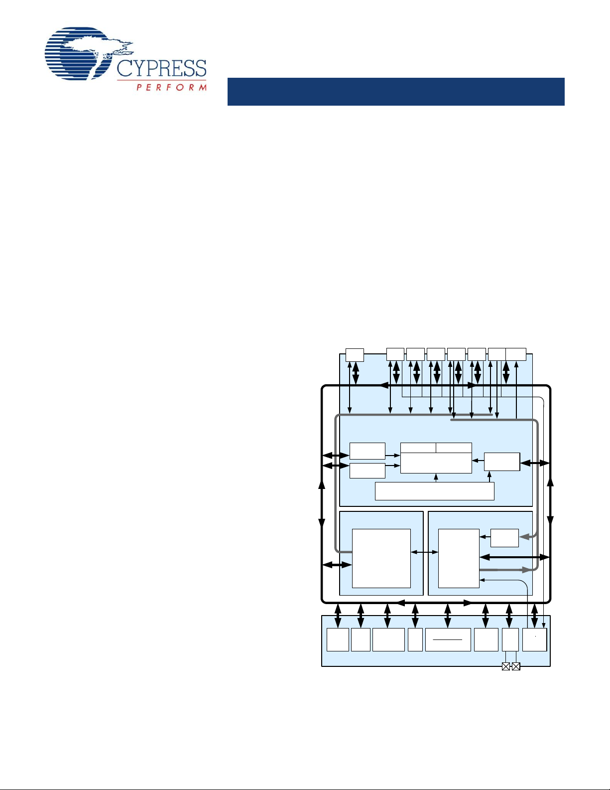
DIGITAL SYSTEM
SRAM
1K
Interrupt
Controller
Sleep and
Watchdog
Clock Sources
(Includes IMO and ILO)
Global Digital Interconnect
Global Analog Interconnect
PSoC CORE
CPU Core (M8C)
SROM Flash 16 KB
Digital
Block
Array
Digital
Clocks
SYSTEM RESOURCES
ANALOG SYSTEM
Analog
Ref.
Port 5 Port 4 Port 3 Port 2 Port 1 Port 0
Analog
Drivers
Analog
Block
Array
Internal
Voltage
Ref.
POR and LVD
System Resets
2
MACs
Decimator
Type 2
I
2
C USB
Port 7
S
y
s
t
e
m
B
u
s
Analog
Input
Muxing
2. Logic Block Diagram
Errata: For information on silicon errata, see “Errata” on page 60. Details include trigger conditions, devices affected, and proposed workaround.
页面指南