
下载
CY8C21123/CY8C21223/CY8C21323
PSoC
®
Programmable System-on-Chip™
Cypress Semiconductor Corporation • 198 Champion Court • San Jose, CA 95134-1709 • 408-943-2600
Document Number: 38-12022 Rev. AC Revised November 22, 2017
Features
■ Powerful Harvard-architecture processor:
❐ M8C processor speeds up to 24 MHz
❐ Low power at high speed
❐ Operating voltage: 2.4 V to 5.25 V
❐ Operating voltages down to 1.0 V using on-chip switch mode
pump (SMP)
❐ Industrial temperature range: –40 °C to +85 °C
■ Advanced peripherals (PSoC
®
blocks):
❐ Four analog type “E” PSoC blocks provide:
• Two comparators with digital to analog converter (DAC)
references
• Single or dual 10-Bit 8-to-1 analog to digital converter
(ADC)
❐ Four digital PSoC blocks provide:
• 8- to 32-bit timers and counters, 8- and 16-bit pulse-width
modulators (PWMs)
• CRC and PRS modules
❐ Full duplex UART, SPI master or slave: Connectable to all
general-purpose I/O (GPIO) pins
❐ Complex peripherals by combining blocks
■ Flexible on-chip memory:
❐ 4 KB flash program storage 50,000 erase/write cycles
❐ 256 bytes SRAM data storage
❐ In-system serial programming (ISSP)
❐ Partial flash updates
❐ Flexible protection modes
❐ EEPROM emulation in flash
■ Complete development tools:
❐ Free development software (PSoC Designer™)
❐ Full-featured, in-circuit emulator (ICE) and programmer
❐ Full-speed emulation
❐ Complex breakpoint structure
❐ 128-KB trace memory
■ Precision, programmable clocking:
❐ Internal ±5% 24- / 48-MHz main oscillator
❐ Internal low-speed, low-power oscillator for watchdog and
sleep functionality
■ Programmable pin configurations:
❐ 25-mA sink, 10-mA source on all GPIOs
❐ Pull-up, pull-down, high Z, strong, or open-drain drive modes
on all GPIOs
❐ Up to eight analog inputs on all GPIOs
❐ Configurable interrupt on all GPIOs
■
■
Additional system resources:
❐ I
2
C master, slave and multi-master to 400 kHz
❐ Watchdog and sleep timers
❐ User-configurable low-voltage detection (LVD)
❐ Integrated supervisory circuit
❐ On-chip precision voltage reference
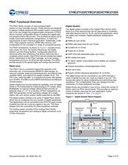
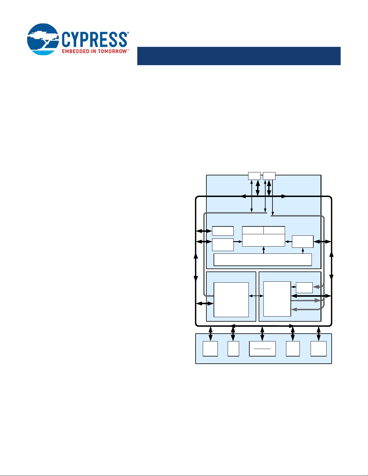
Logic Block Diagram
DIGITAL SYSTEM
SRAM
System Bus
Int er rupt
Controller
Sleep and
Watchdog
Clock Sources
(Includes IMO and ILO)
Global Digital Interconnect
Global Analog Interconnect
PSoC
CORE
CPU Core
(M8C)
SROM Flas h
I2C
Internal
Voltage
Ref .
Digit al
Cloc ks
POR and LVD
System Resets
SYSTEM RESOURCES
ANALOG SYSTEM
Analog
Ref .
Por t 1 Por t 0
Digita l
P S o C B l oc k
Array
Ana log
PSoC Block
Array
Sw itch
Mode
Pu mp
Errata: When the device is operated within 0 °C to 70 °C, the frequency tolerance is reduced to ±2.5%, but if operated at extreme temperature (below 0 °C or above 70 °C),
frequency tolerance deviates from ±2.5% to ±5%. For information on silicon errata, see “Errata” on page 43.
页面指南