


下载
CY25402/CY25422/CY25482
Two PLL Programmable Clock Generator
with Spread Spectrum
Cypress Semiconductor Corporation • 198 Champion Court • San Jose, CA 95134-1709 • 408-943-2600
Document Number: 001-12565 Rev. *I Revised December 3, 2014
Two PLL Programmable Clock Generator with Spread Spectrum
Features
■ Two fully integrated phase locked loops (PLLs)
■ Input frequency range
❐ External crystal: 8 to 48 MHz
❐ External reference: 8 to 166 MHz clock
■ Reference clock input voltage range
❐ 2.5 V, 3.0 V, and 3.3 V for CY25482
❐ 1.8 V for CY25402 and CY25422
■ Wide operating output frequency range
❐ 3 to 166 MHz
■ Programmable
[1]
spread spectrum with center and down
spread option and lexmark and linear modulation profiles
■ V
DD
supply voltage options:
❐ 2.5 V, 3.0 V, and 3.3 V for CY25402 and CY25482
❐ 1.8 V for CY25422
■ Selectable output clock voltages independent of V
DD
:
❐ 2.5 V, 3.0 V, and 3.3 V for CY25402 and CY25482
❐ 1.8 V for CY25422
■ Frequency select feature with option to select four different
frequencies
■ Power-down, Output Enable, and SS ON/OFF controls
■ Low jitter, high accuracy outputs
■ Ability to synthesize nonstandard frequencies with Fractional-N
capability
■ Three clock outputs with programmable drive strength
■ Glitch-free outputs while frequency switching
■ 8-pin small outline integrated circuit (SOIC) package
■ Commercial and Industrial temperature ranges
Benefits
■ Multiple high performance PLLs allow synthesis of unrelated
frequencies
■ Nonvolatile programming for personalization of PLL
frequencies, spread spectrum characteristics, drive strength,
crystal load capacitance, and output frequencies
■ Application specific programmable EMI reduction using spread
spectrum for clocks
■ Programmable PLLs for system frequency margin tests
■ Meets critical timing requirements in complex system designs
■ Suitability for PC, consumer, portable, and networking
applications
■ Capable of zero parts per million (PPM) frequency synthesis
error
■ Uninterrupted system operation during clock frequency switch
■ Application compatibility in standard and low power systems
■ For a complete list of related documentation, click here.
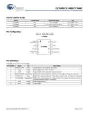
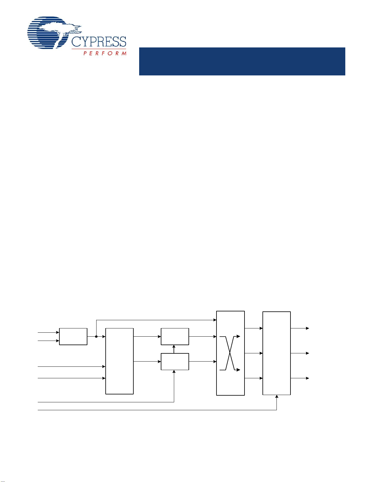
Block Diagram
OSC
CLK2
REFOUT
CLK1
Crossbar
Switch
FS1
SSON
XOUT
XIN/
EXCLKIN
PD#/OE
PLL 2
(SS)
FS0
MUX
and
Control
Logic
PLL 1
(SS)
Output
Dividers
and
Drive
Strength
Control
页面指南