
下载

8-Bit Programmable 2- to 5-Phase
Synchronous Buck Controller
ADP3189
FEATURES
Selectable 2-, 3-, 4-, or 5-phase operation at up
to 1 MHz per phase
±7.7 mV worst-case differential sensing error over
temperature
Logic-level PWM outputs for interface to external
high-power drivers
Active current balancing between all output phases
Built-in power good/crowbar blanking supports on-the-fly
VID code changes
Digitally programmable 0.5 V to 1.6 V output— supports
both VR10.x and VR11 specifications
Programmable short-circuit protection with programmable
latch-off delay
APPLICATIONS
Desktop PC power supplies for
Next generation Intel® processors
VRM modules
GENERAL DESCRIPTION
The ADP3189
1
is a highly efficient multi-phase synchronous
buck switching regulator controller optimized for converting a
12 V main supply into the core supply voltage required by high
performance Intel processors. It uses an internal 8-bit DAC
to read a voltage identification (VID) code directly from the
processor, which is used to set the output voltage between 0.5 V
and 1.6 V.
For more information about the ADP3189, contact
Analog Devices via email at
mary.burke@analog.com
and
lee.space@analog.com.
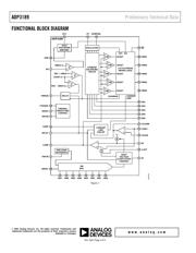
This device uses a multi-mode PWM architecture to drive the
logic-level outputs at a programmable switching frequency that
can be optimized for VR size and efficiency. The phase relation-
ship of the output signals can be programmed to provide 2-, 3-,
4-, or 5-phase operation, allowing for the construction of up to
five complementary buck switching stages.
The ADP3189 also includes programmable no-load offset and
slope functions to adjust the output voltage as a function of the
load current, so it is optimally positioned for a system transient.
The ADP3189 also provides accurate and reliable short-circuit
protection, adjustable current limiting, and a delayed power
good output that accommodates on-the-fly output voltage
changes requested by the CPU.
ADP3189 is specified over the extended commercial tem-
perature range of 0°C to +85°C and is available in a
40-lead LFCSP package.
1
Protected by U.S. Patent Number 6,683,441; others pending.
Rev. Sp0
Information furnished by Analog Devices is believed to be accurate and reliable. However, no
responsibility is assumed by Analog Devices for its use, nor for any infringements of patents or other
rights of third parties that may result from its use. Specifications subject to change without notice. No
license is granted by implication or otherwise under any patent or patent rights of Analog Devices.
Trademarks and registered trademarks are the property of their respective owners.
One Technology Way, P.O. Box 9106, Norwood, MA 02062-9106, U.S.A.
Tel: 781.329.4700 www.analog.com
Fax: 781.461.3113 © 2005 Analog Devices, Inc. All rights reserved.