
下载
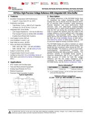
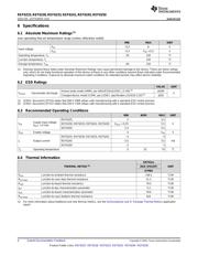
±4
±3
±2
±1
0
1
2
3
4
0 200 400 600 800 1000
Reference Droop (LSB)
Time (µs)
C04
Regular Voltage Reference Droop
REF62xx Droop
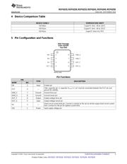
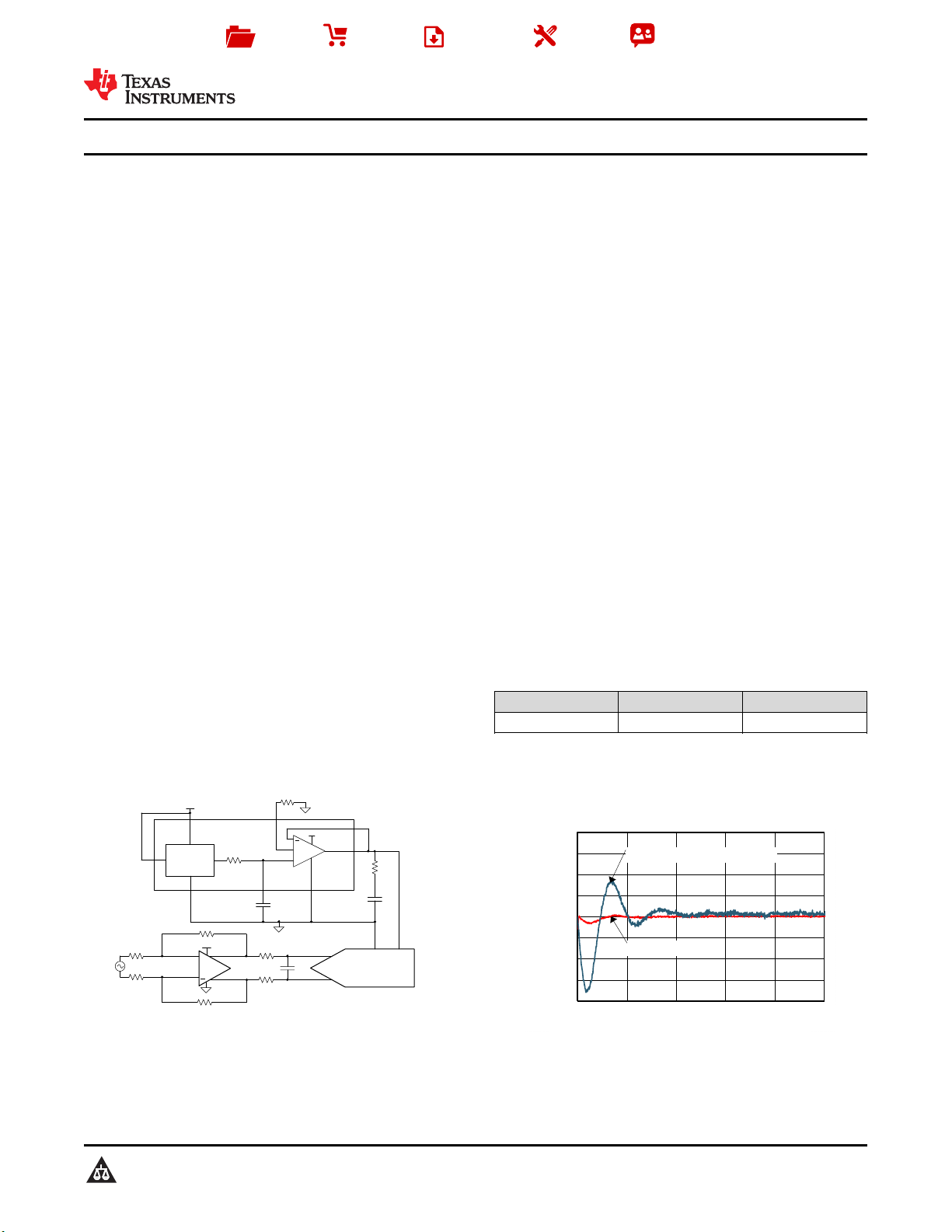
Bandgap
Voltage
Reference
C
FILT
C
L
R
ESR
R
FILT
Buffer
+
VIN
OUT_S
OUT_F
FILT
VIN
GND_S GND_F
Power Supply
SS
REF62xx
R
LIM
EN
GND
REF
+
V
IN
R
R
R
Power Supply
R
F
R
F
R
C
F
THS4521
AINP
AINN
ADS8881
Copyright © 2016, Texas Instruments Incorporated
Product
Folder
Sample &
Buy
Technical
Documents
Tools &
Software
Support &
Community
An IMPORTANT NOTICE at the end of this data sheet addresses availability, warranty, changes, use in safety-critical applications,
intellectual property matters and other important disclaimers. PRODUCTION DATA.
REF6225
,
REF6230
,
REF6233
,
REF6241
,
REF6245
,
REF6250
SBOS748 –SEPTEMBER 2016
REF62xx High-Precision Voltage Reference With Integrated ADC Drive Buffer
1
1 Features
1
• Excellent Temperature Drift Performance
– 3 ppm/°C (max) from 0°C to +70°C
• Extremely Low Noise
– Total Noise: 5 µV
RMS
With 47-µF Capacitor
– 1/f Noise (0.1 Hz to 10 Hz): 3 µV
PP
/V
• Integrated ADC Drive Buffer
– Low Output Impedance: < 50 mΩ (0-200 kHz)
– First Sample Precise to 18 Bits With ADS8881
– Enables Burst-Mode DAQ Systems
• Low Supply Current: 820 μA
• Low Shutdown Current: 1 µA
• High Initial Accuracy: ±0.05%
• Very-Low Noise and Distortion
– SNR: 100.5 dB, THD: –125 dB (ADS8881)
– SNR: 106 dB, THD: –120 dB (ADS127L01)
• Output Current Drive: ±4 mA
• Programmable Short-Circuit Current
• Verified to Drive REF Pin of ADS88xx family of
SAR ADCs and ADS127xx family of Wideband ΔΣ
ADCs
2 Applications
• ATE Testers and Oscilloscopes
• Test and Measurement Equipment
• Analog Input Modules for PLCs
• Medical Equipment
• Precision Data Acquisition Systems
3 Description
The voltage references in the REF6000 family have
an integrated low output impedance buffer that
enables the user to directly drive the reference (REF)
pin of precision data converters, while preserving
linearity, distortion, and noise performance. Most
precision SAR and delta-sigma analog-to-digital
converters (ADCs), switch binary-weighted capacitors
onto the REF pin during the conversion process. In
order to support this dynamic load, the output of the
voltage reference must be buffered with a low-output
impedance, high-bandwidth buffer. The REF6000
family devices are well suited, but not limited, to drive
the REF pin of the ADS88xx family of SAR ADCs,
and ADS127xx family of delta-sigma ADCs, as well
as precision digital-to-analog converters (DACs).
The REF6000 family of is able to maintain an output
voltage within 1LSB (18-bit) with minimal droop, even
during the first conversion while driving the REF pin
of the ADS8881. This feature is useful in burst-mode,
event-triggered, equivalent-time sampling, and
variable-sampling-rate data-acquisition systems. The
REF62xx variants of REF6000 family specify a
maximum temperature drift of just 3 ppm/°C and
initial accuracy of 0.05% for both the voltage
reference and the low output impedance buffer
combined. For various temperature drift options in
REF6000 family, see the Device Comparison Table.
Device Information
(1)
PART NUMBER PACKAGE BODY SIZE (NOM)
REF62xx VSSOP (8) 3.00 mm x 3.00 mm
(1) For all available packages, see the package option addendum
at the end of the data sheet.
Typical Application
Reference Droop comparison
(1 LSB = 19.07 µV, With ADS8881 at 1 MSPS)
页面指南