

下载
© 2007 Microchip Technology Inc. DS22072A-page 1
MCP3425
Features
• 16-bit ΔΣ ADC in a SOT-23-6 package
• Differential input operation
• Self calibration of Internal Offset and Gain per
each conversion
• On-board Voltage Reference:
- Accuracy: 2.048V ± 0.05%
• On-board Programmable Gain Amplifier (PGA):
- Gains of 1,2, 4 or 8
• On-board Oscillator
• INL: 10 ppm of FSR (FSR = 4.096V/PGA)
• Programmable Data Rate Options:
- 15 SPS (16 bits)
- 60 SPS (14 bits)
- 240 SPS (12 bits)
• One-Shot or Continuous Conversion Options
• Low current consumption:
- 145 µA typical
(V
DD
= 3V, Continuous Conversion)
• One-Shot Conversion (1 SPS) with V
DD
= 3V:
- 9.7 µA typical with 16 bit mode
- 2.4 µA typical with 14 bit mode
- 0.6 µA typical with 12 bit mode
• Supports I
2
C Serial Interface:
- Standard, Fast and High Speed Modes
• Single Supply Operation: 2.7V to 5.5V
• Extended Temperature Range: -40°C to 125°C
Typical Applications
• Portable Instrumentation
• Weigh Scales and Fuel Gauges
• Temperature Sensing with RTD, Thermistor, and
Thermocouple
• Bridge Sensing for Pressure, Strain, and Force.
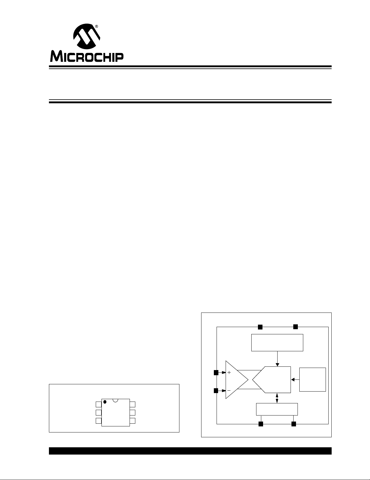
Package Types
Description
The MCP3425 is a single channel low-noise, high
accuracy ΔΣ A/D converter with differential inputs and
up to 16 bits of resolution in a small SOT-23-6 package.
The on-board precision 2.048V reference voltage
enables an input range of ±2.048V differentially
(Δ voltage = 4.096V). The device uses a two-wire I
2
C
compatible serial interface and operates from a single
2.7V to 5.5V power supply.
The MCP3425 device performs conversion at rates of
15, 60, or 240 samples per second (SPS) depending
on the user controllable configuration bit settings using
the two-wire I
2
C serial interface. This device has an on-
board programmable gain amplifier (PGA). The user
can select the PGA gain of x1, x2, x4, or x8 before the
analog-to-digital conversion takes place. This allows
the MCP3425 device to convert a smaller input signal
with high resolution. The device has two conversion
modes: (a) Continuous mode and (b) One-Shot mode.
In One-Shot mode, the device enters a low current
standby mode automatically after one conversion. This
reduces current consumption greatly during idle peri-
ods.
The MCP3425 device can be used for various high
accuracy analog-to-digital data conversion applications
where design simplicity, low power, and small footprint
are major considerations.
Block Diagram
1
2
3
4
5
6
V
IN
+
V
SS
SCL
V
IN
-
V
DD
SDA
Top View
SOT-23-6
V
SS
V
DD
V
IN
+
V
IN
-
SCL
SDA
Voltage Reference
Clock
(2.048V)
I
2
C Interface
Gain = 1, 2, 4, or 8
V
REF
ΔΣ ADC
Converter
PGA
Oscillator
1 6- Bi t A nal og -t o- Di gi ta l C on ve rt er
with I
2
C Interface and On-Board Reference
页面指南