

下载

1
SLAU547B–January 2014–Revised April 2016
Submit Documentation Feedback
Copyright © 2014–2016, Texas Instruments Incorporated
DAC3XJ8XEVM
User's Guide
SLAU547B–January 2014–Revised April 2016
DAC3XJ8XEVM
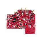
The DAC3XJ8XEVM is an evaluation module (EVM) designed to evaluate the DAC3XJ8X family of high-
speed, JESD204B interface DACs (DAC37J82, DAC37J84, DAC38J82, DAC38J84, DAC39J82,
DAC39J84). The EVM includes an onboard clocking solution (LMK04828), transformer coupled outputs,
full power solution, and easy-to-use software GUI and USB interface.
The DAC3XJ8XEVM is designed to work seamlessly with the TSW14J56EVM, Texas Instruments’
JESD204B pattern generator card, through the High Speed Data Converter Pro (HSDCPro) software tool
for high-speed data converter evaluation. The DAC3XJ8XEVM was also designed to work with many of
the development kits from leading FPGA vendors that contain an FMC connector.
Contents
1 Functional Description....................................................................................................... 2
2 Schematics, Layout, and BOM............................................................................................. 3
3 Software Control ............................................................................................................. 3
3.1 Installation Instructions............................................................................................. 3
3.2 Software Operation................................................................................................. 4
4 Basic Test Setup............................................................................................................. 8
4.1 Test Block Diagram................................................................................................. 8
4.2 TSW14J56 Setup ................................................................................................... 8
4.3 DAC3XJ8X Quick-Start Procedure ............................................................................... 9
5 Clock Configuration ........................................................................................................ 14
5.1 DAC3XJ8XEVM Clocking Options.............................................................................. 14
5.2 LMK04828 Configuration Options............................................................................... 15
6 References.................................................................................................................. 15
List of Figures
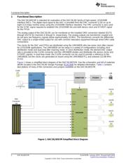
1 DAC3XJ8XEVM Simplified Block Diagram............................................................................... 2
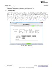
2 Quick Start Page............................................................................................................. 4
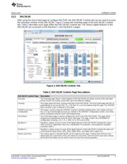
3 DAC3XJ8X Controls Tab ................................................................................................... 5
4 LMK04828 Controls Tab.................................................................................................... 6
5 Low Level View Tab......................................................................................................... 7
6 Test Setup .................................................................................................................... 8
7 DAC3XJ8X GUI Configuration for DAC37J82, DAC38J82, and DAC39J82 ....................................... 11
8 DAC3XJ8X GUI Configuration for DAC37J84, DAC38J84, and DAC39J84 ....................................... 12
9 Spectrum Analyzer Example.............................................................................................. 13
List of Tables
1 Input and Output Connectors and Jumper Descriptions................................................................ 3
2 DAC3XJ8X Controls Page Descriptions .................................................................................. 5
3 LMK04828 Controls Page Descriptions................................................................................... 6