

下载
Quick Start Guide
SLWU070C–February 2010–Revised March 2013
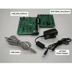
TSW6011EVM
This document outlines the basic steps and functions that are required for the proper operation of the
TSW6011 evaluation module (EVM) system. The TSW6011EVM is a single RX channel board that can be
used to demonstrate a TRF371125 integrated direct downconversion receiver interfacing to an ADS5282
octal analog-to-digital converter (ADC). This guide helps the user to evaluate the performance of various
modes of operation of the TSW6011EVM. Throughout this document, the term evaluation module and the
abbreviation EVM are synonymous with the TSW6011EVM.
Contents
1 Overview ..................................................................................................................... 2
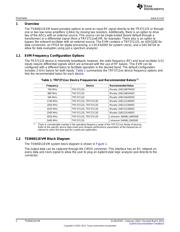
1.1 EVM Frequency Configuration Options ......................................................................... 2
1.2 TSW6011EVM Block Diagram ................................................................................... 2
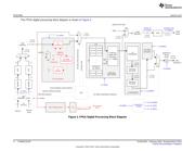
1.3 Digital Processing Block Functions .............................................................................. 3
2 Software Installation ........................................................................................................ 5
2.1 Installation Instructions ............................................................................................ 5
3 EVM Test Configuration .................................................................................................... 5
3.1 Test Equipment ..................................................................................................... 5
3.2 Calibration ........................................................................................................... 5
4 Board Bring Up .............................................................................................................. 6
4.1 Power Up ............................................................................................................ 6
4.2 Basic RF Test ...................................................................................................... 7
4.3 Software Operation ................................................................................................ 8
4.4 Device Initialization ................................................................................................ 9
5 TR371125 Register Definitions .......................................................................................... 14
5.1 Register 1 .......................................................................................................... 14
5.2 Register 2 .......................................................................................................... 14
5.3 Register 3 .......................................................................................................... 14
5.4 Register 5 .......................................................................................................... 14
Appendix A ....................................................................................................................... 15
List of Figures
1 TSW6011EVM System Block Diagram .................................................................................. 3
2 FPGA Digital Processing Block Diagram ................................................................................ 4
3 TSW6011EVM Board Top View .......................................................................................... 7
4 TSW6011EVM Software GUI Front Panel............................................................................... 8
5 GUI Communication Error ................................................................................................. 8
6 ADS5282 Control Panel.................................................................................................... 9
7 TR371125 Control Panel ................................................................................................. 10
8 Test Tone From DAC5672 Output ...................................................................................... 11
9 Digital Processing Control Panel ........................................................................................ 12
10 Test Tone After IQ Correction and DC Offset Compensation ...................................................... 13
All trademarks are the property of their respective owners.
1
SLWU070C–February 2010–Revised March 2013 TSW6011EVM
Submit Documentation Feedback
Copyright © 2010–2013, Texas Instruments Incorporated