

下载

AP4310A
Document number: DS36510 Rev. 2 - 2
1 of 8
www.diodes.com
September 2014
© Diodes Incorporated
AP4310A
A Product Line of
Diodes Incorporated
DUAL OP AMP AND VOLTAGE REFERENCE
Description
The AP4310A is a monolithic IC specifically designed to regulate the
output current and voltage levels of switching battery chargers and
power supplies
The device contains two Op Amps and a 2.5V precision shunt voltage
reference. Op Amp 1 is designed for voltage control with its non-
inverting input internally connected to the output of the shunt
regulator. Op Amp 2 is for current control with both inputs
uncommitted. The IC offers the power converter designer a control
solution that features increased precision with a corresponding
reduction in system complexity and cost.
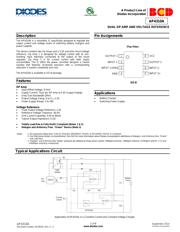
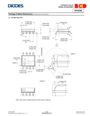
The AP4310A is available in SO-8 package.
Features
OP Amp
Input Offset Voltage: 0.5mV
Supply Current: 75A per OP Amp at 5.0V Supply Voltage
Unity Gain Bandwidth:1MHz
Output Voltage Swing: 0 to V
CC
-1.5V
Power Supply Range: 3 to 36V
Voltage Reference
Fixed Output Voltage Reference: 2.5V
Reference Voltage Tolerance :±0.4%
Sink Current Capability: 0.05 to 80mA
Typical Output Impedance: 0.2Ω
Totally Lead-free & Fully RoHS Compliant (Notes 1 & 2)
Halogen and Antimony Free. “Green” Device (Note 3)
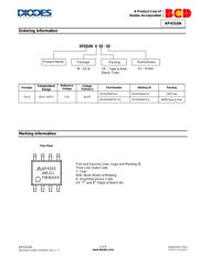
Pin Assignments
(Top View)
SO-8
Applications
Battery Charger
Switching Power Supply
Notes: 1. No purposely added lead. Fully EU Directive 2002/95/EC (RoHS) & 2011/65/EU (RoHS 2) compliant.
2. See http://www.diodes.com/quality/lead_free.html for more information about Diodes Incorporated’s definitions of Halogen- and Antimony-free, "Green"
and Lead-free.
3. Halogen- and Antimony-free "Green” products are defined as those which contain <900ppm bromine, <900ppm chlorine (<1500ppm total Br + Cl) and
<1000ppm antimony compounds.
Typical Applications Circuit
AC
Line
SMPS
R2
Current
Sense
R7
R8
Battery
Pack
R4
R3
R5
R6
R1
Opto
Isolator
+
-
Op Amp 2
+
-
Op Amp 1
AP4310A
V
REF
Application of AP4310A in a Constant Current and Constant Voltage Charger
1
2
3
4
8
7
6
5
OUTPUT 1
INPUT 1-
INPUT 1+/VKA
VCC
OUTPUT 2
INPUT 2-
INPUT 2+
GND
页面指南