
下载
PRODUCTPREVIEW
AM3874, AM3872, AM3871
www.ti.com
SPRS695A –SEPTEMBER 2011–REVISED MARCH 2012
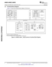
AM387x Sitara™
ARM® Processors
Check for Samples: AM3874, AM3872, AM3871
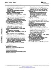
1 High-Performance System-on-Chip (SoC)
1.1 Features
12
• One 8-bit Only Input
• High-Performance Sitara™ ARM® Processors
– Two 165 MHz HD Video Display Outputs
– Up to 1-GHz ARM® Cortex™-A8 RISC Core
• One 16/24/30-bit and one 16/24-bit Output
• ARM® Cortex™-A8 Core
– Composite or S-Video Analog Output
– ARMv7 Architecture
– MacroVision® Support Available
• In-Order, Dual-Issue, Superscalar
Processor Core – Digital HDMI 1.3 transmitter With Integrated
PHY
• NEON™ Multimedia Architecture
– Advanced Video Processing Features Such
• Supports Integer and Floating Point
as Scan/Format/Rate Conversion
• Jazelle® RCT Execution Environment
– Three Graphics Layers and Compositors
• ARM® Cortex™-A8 Memory Architecture
• Dual 32-bit LPDDR/DDR2/DDR3 SDRAM
– 32K-Byte Instruction and Data Caches
Interfaces
– 512K-Byte L2 Cache
– Supports up to LPDDR-400, DDR2-800, and
– 64K-Byte RAM, 48K-Byte Boot ROM
DDR3-800
• 128K-Bytes On-Chip Memory Controller
– Up to Eight x 8 Devices Total 2 GB Total
(OCMC) RAM
Address Space
• Imaging Subsystem (ISS)
– Dynamic Memory Manager (DMM)
– Camera Sensor Connection
• Programmable Multi-Zone Memory
• Parallel Connection for Raw (up to 16-Bit)
Mapping and Interleaving
and BT.656/BT.1120 (8-/16-bit)
• Enables Efficient 2D Block Accesses
– Image Sensor Interface (ISIF) for Handling
• Supports Tiled Objects in 0°, 90°, 180°, or
Image/Video Data From the Camera Sensor
270° Orientation and Mirroring
– Resizer
• Optimizes Interlaced Accesses
• Resizing Image/Video From 1/16x to 8x
• General Purpose Memory Controller (GPMC)
• Generating Two Different Resizing
– 8-/16-bit Multiplexed Address/Data Bus
Outputs Concurrently
– 512M-Byte Total Address Space Divided
• Media Controller
Among up to 8 Chip Selects
– Controls the HDVPSS and ISS
– Glueless Interface to NOR Flash, NAND
• SGX530 3D Graphics Engine
Flash (BCH/Hamming Error Code Detection),
– Delivers up to 25 MPoly/sec
SRAM and Pseudo-SRAM
– Universal Scalable Shader Engine
– Error Locator Module (ELM) Outside of
– Direct3D Mobile, OpenGLES 1.1 and 2.0,
GPMC to Provide Upto 16-Bit/512-Bytes
OpenVG 1.0, OpenMax API Support
Hardware ECC for NAND
– Advanced Geometry DMA Driven Operation
– Flexible Asynchronous Protocol Control for
Interface to FPGA, CPLD, ASICs, etc.
– Programmable HQ Image Anti-Aliasing
• Enhanced Direct-Memory-Access (EDMA)
• Endianness
Controller
– ARM Instructions/Data – Little Endian
– Four Transfer Controllers
• HD Video Processing Subsystem (HDVPSS)
– 64/8 Independent DMA/QDMA Channels
– Two 165 MHz HD Video Capture Inputs
• Dual Port Ethernet (10/100/1000 Mb/s) With
• One 16/24-bit Input, Splittable into Dual 8-
Optional Switch
bit SD Capture Ports
– IEEE 802.3 Compliant (3.3V I/O Only)
• One 8/16/24-bit Input
1
Please be aware that an important notice concerning availability, standard warranty, and use in critical applications of
Texas Instruments semiconductor products and disclaimers thereto appears at the end of this data sheet.
2All trademarks are the property of their respective owners.
PRODUCT PREVIEW information concerns products in the formative or design phase of
Copyright © 2011–2012, Texas Instruments Incorporated
development. Characteristic data and other specifications are design goals. Texas
Instruments reserves the right to change or discontinue these products without notice.
页面指南