
下载
AN3789
1
RF Application Information
Freescale Semiconductor
Clamping of High Power RF Transistors and
RFICs in Over-Molded Plastic Packages
By: Mahesh Shah, Richard Rowan, Lu Li, Quan Li, Eddie Mares, and Leonard Pelletier
INTRODUCTION
This application note provides Freescale Semiconductor
customers with a guide for mounting high power RF
transistors and integrated circuits in Over-Molded Plastic
(OMP) packages by clamping down the RF power device in
the Power Amplifier (PA) housing. Each PA design has its
own unique characteristics. Similarly, each manufacturing
operation also has its own process capabilities and
variations. Therefore, each design and assembly may
require some fine-tuning. The intent of this application note
is to provide customers with the information necessary to
derive the best possible process that is most suitable for their
design and the assembly process that is most compatible
with their manufacturing operation.
The RF Power devices are generally assembled into the
PA assembly by either a solder reflow process (including
surface mounting) or a bolt-down process through an
opening in the Printed Circuit Board (PCB). Soldering the
devices provides a very good thermal and electrical
grounding due to the high conductivity interface of a solder
joint, which results in improved RF performance. The PA is
also less susceptible to oscillation type damage when it is
properly grounded. Better thermal grounding also results in
lower junction temperature and higher reliability. For
customers who rely on bolting the RF power devices in the
housing, there is usually some degradation in performance
as well as stability and reliability. This is primarily due to
variation in source impedance from one installation to
another as well as poor interface resistance. As a result, the
PA industry has seen a steady shift away from bolt-down to
solder reflow mounting.
However, some customers still prefer bolting down RF
Power devices. This application note provides guidelines for
those customers who would like to improve the performance
of their PAs using the bolt-down type process.
This application note describes the methodology to design
an injection molded clamp that clamps the device body only.
The leads are soldered to the PCB. Freescale’s testing of a
properly designed clamp showed an improvement in the
area of contact between the device source contact and the
aluminum chassis in which the PA is housed. This improved
thermal and electrical grounding increased the performance
of OMP devices in the PA assembly.
Based on the guidelines presented here, customers
should be able to develop a manufacturable assembly
process that can do the following:
• Design a clamp that will fit into their assembly.
• Provide a good thermal ground to conduct the dissipated
heat efficiently from the high power RF device to the
system sink.
• Provide a good electrical ground to provide a stable RF
performance over the life of the power transistor.
• Maintain the package integrity during the assembly and in
the field.
• Design a system where reflowed and clamped devices will
not compromise solder joint reliability.
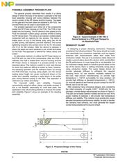
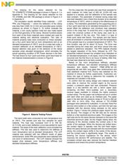
Figure 1. Typical RF Power Device in an
Over-Molded Plastic (OMP) Package Suitable for
Clamp-Down Assembly Operation
The TO-270WB device shown in Figure 1 is designed to
be reflowed into a cavity with the source contact soldered to
a pallet or coin and the leads soldered to the PCB. The
method described here is applicable to all OMP devices
where the source contact is not soldered but is held in
physical contact by the clamping force.
AN3789
Rev. 0, 3/2009
Freescale Semiconductor
Application Note
Freescale Semiconductor, Inc., 2009. All rights reserved.