

下载

User's Guide
SLAU467A–November 2012–Revised August 2013
ADS42JB46, ADS42JB49, and ADS42JB69 Evaluation
Module
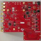
This document outlines the basic steps and functions that are required to ensure the proper operation of
the Texas Instruments (TI) ADS42JB46, ADS42JB49, and ADS42JB69 Evaluation Modules (hereafter in
this document, ADS42JBxxEVM or EVM). The EVM includes an ADS42JBxxEVM, a 5-VDC power supply,
and a mini-USB cable. This EVM is designed to be used with a JESD204B capture card using a FMC
connector interface such as the TI JESD204B Translation card and TSW1400EVM or a FPGA
development board, such as the Xilinx KC705. The ADS42JBxxEVM contains either an ADS42JB49 (14-
bit), or ADS42JB69 (16-bit) dual-channel, 250-MSPS, or an ADS42JB46 (14-bit) dual channel, 160-MSPS
analog-to-digital converter. The EVM also contains a TI LMK04828 clock jitter cleaner. When used with a
TI JESD204B Translation card, JESD204B standard output data from the EVM is captured and translated
into parallel LVDS data then sent to the TSW1400 for analysis. This guide helps users to quickly evaluate
the performance of the ADS42JBxxEVM boards by capturing and displaying waveforms using the
TSW1400High Speed Data Converter Pro GUI software. The EVM schematics, BOMs, and layout files are
found in the design package under the ADS42JBxxEVM product folder on www.ti.com.
Contents
1 Introduction .................................................................................................................. 2
1.1 Overview ............................................................................................................ 2
1.2 Block Diagram ...................................................................................................... 2
2 Software Control ............................................................................................................ 3
2.1 Installation Instructions ............................................................................................ 3
2.2 Software Operation ................................................................................................ 4
3 Basic Test Setup .......................................................................................................... 13
3.1 Test Block Diagram .............................................................................................. 13
3.2 TSW1400EVM Setup ............................................................................................ 15
3.3 ADS42JBxxEVM Quick-Start Procedure ...................................................................... 15
List of Figures
1 Block Diagram of the ADS42JBxxEVM .................................................................................. 2
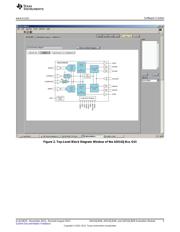
2 Top-Level Block Diagram Window of the ADS42JBxx GUI ........................................................... 5
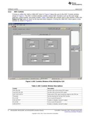
3 ADC Controls Window of the ADS42JBxx GUI ......................................................................... 6
4 Digital Block Controls Window of the ADS42JBxx GUI................................................................ 7
5 JESD204B Controls Window of the ADS42JBxx GUI.................................................................. 8
6 LMK04828 Outputs Control Window of the ADS42JBxx GUI......................................................... 9
7 LMK04828 Input Clock Settings......................................................................................... 10
8 LMK04828 PLL1 Controls................................................................................................ 11
9 LMK04828 PLL2 Controls................................................................................................ 12
10 LMK04828 SYSREF Settings............................................................................................ 13
11 Test Setup.................................................................................................................. 14
12 High Speed Data Converter Pro (HSDCPro) Sample Capture...................................................... 17
List of Tables
1 Input and Output Connectors and Jumper Descriptions of the ADS42JBxxEVM .................................. 3
2 ADC Controls Window Descriptions...................................................................................... 6
Windows is a registered trademark of Microsoft Corporation.
1
SLAU467A–November 2012–Revised August 2013 ADS42JB46, ADS42JB49, and ADS42JB69 Evaluation Module
Submit Documentation Feedback
Copyright © 2012–2013, Texas Instruments Incorporated