

下载

User's Guide
SLAU579C–June 2014–Revised January 2016
ADC3xxx, ADC3xJxx EVM User’s Guide
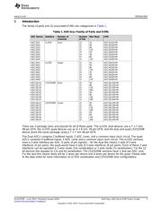
This document is intended to serve as a user’s guide for the ADC3xxx EVM and ADC3xJxx EVM. The
EVMs provide a platform for evaluating the ADC3xxx which is a dual- or quad-channel, 12- or 14-bit serial
LVDS interface, analog-to-digital converter (ADC) with sampling speed grades of 25, 50, 80, and 125
Msps. The ADC3xJxx is a dual- or quad-channel, 12- or 14-bit JESD204B-compliant interface ADC with
sampling speed grades of 50, 80, 125, and 160 Msps. This family of converters only requires a single 1.8-
V supply, provides flexible input clock dividers, and provides internal features for improved 1/f (ADC32xx,
ADC34xx) and SFDR performance. Throughout this document, the abbreviations EVM and ADC3xxxx,
and the term evaluation module are synonymous with the ADC3xxx EVM and ADC3xJxx EVM, unless
otherwise noted.
Contents
1 Introduction ................................................................................................................... 3
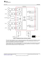
1.1 EVM Block Diagram................................................................................................ 4
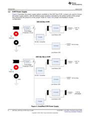
1.2 EVM Power Supply................................................................................................. 6
1.3 EVM Connectors and Jumpers ................................................................................... 7
1.4 EVM ADC Input Circuit Configurations......................................................................... 10
2 Software Control............................................................................................................ 12
2.1 Installation Instructions ........................................................................................... 12
2.2 Software Operation ............................................................................................... 12
3 Basic Test Procedure...................................................................................................... 21
3.1 Test Block Diagram with ADC32xx and ADC34xx............................................................ 21
3.2 Test Set-up Connection .......................................................................................... 22
3.3 ADC32/34xx and TSW1400 Setup Guide...................................................................... 22
3.4 Test Block Diagram with ADC32Jxx and ADC34Jxx ......................................................... 24
3.5 Test Set-up Connection (Onboard LMK04828 Clock)........................................................ 25
3.6 ADC32J/34Jxx and TSW14J56 Setup Guide.................................................................. 26
List of Figures
1 Simplified ADC344x EVM Block Diagram ................................................................................ 4
2 Simplified ADC34J4x EVM Block Diagram............................................................................... 5
3 Simplified EVM Power Supply ............................................................................................. 6
4 ADC34Jxx EVM Connector and Jumper Locations ..................................................................... 7
5 ADC34xx EVM Connector and Jumper Locations ...................................................................... 8
6 ADC3xxxx ADC Input Circuit options.................................................................................... 11
7 DC34xx Clock Input Circuit ............................................................................................... 11
8 Common Tab ............................................................................................................... 13
9 ADC32xx Tab............................................................................................................... 14
10 ADC34XX Tab.............................................................................................................. 16
11 ADC32Jxx Tab.............................................................................................................. 18
12 ADC34Jxx Tab.............................................................................................................. 20
13 ADC32xx/ADC34xx and TSW1400 Test Setup Block Diagram...................................................... 21
14 Select ADC32xx or 34xx in the HSDC Pro GUI Program............................................................. 22
15 ADC3xxx Operating in 14-Bit Mode at 125 Msps with 10-MHz Input Signal....................................... 23
16 ADC32Jxx/ADC34Jxx and TSW14J56 Test Setup Block Diagram.................................................. 24
All trademarks are the property of their respective owners.
1
SLAU579C–June 2014–Revised January 2016 ADC3xxx, ADC3xJxx EVM User’s Guide
Submit Documentation Feedback
Copyright © 2014–2016, Texas Instruments Incorporated