


下载

1
www.pericom.com P-0.1 04/27/11
PI6C20800B
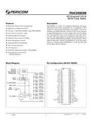
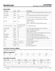
Block Diagram Pin Configuration (48-Pin TSSOP)
Description
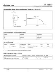
PI6C20800B is a PCIe 3.0 compliant, high-speed, low-noise
differential clock buffer designed to be a companion to PCI
Express 3.0 clock generator for Intel server chipsets. The device
distributes the differential SRC clock from PCIe clock generator
to eight differential pairs of clock outputs either with or without
PLL. The input SRC clock can be divided by 2 when SRC_DIV#
is LOW. The clock outputs are controlled by input selection of
SRC_STOP#, PWRDWN# and SMBus, SCLK and SDA. When
input of either SRC_STOP# or PWRDWN# is LOW, the output
clocks are Tristated. When PWRDWN# is LOW, the SDA and
SCLK inputs must be Tristated.
Features
Î Phase jitter lter for PCIe 3.0 application
Î Eight Pairs of Dierential Clocks
Î Low skew < 50ps (PI6C20800B), <60ps (PI6C20800BI)
Î Low Cycle-to-cycle jitter < 60ps
Î Output Enable for all outputs
Î Outputs Tristate control via SMBus
Î Power Management Control
Î Programmable PLL Bandwidth
Î PLL or Fanout operation
Î 3.3V Operation
Î Industrial Temperature Option - PI6C20800BI
Î Packaging (Pb-Free & Green):
— 48-Pin TSSOP (A)
PCI Express® 3.0 1:8
HCSL Clock Buffer
OUT0
OUT0#
OUT1
OUT1#
OUT2
OUT2#
OUT3
OUT3#
DIV
Output
Control
SMBus
Controller
PLL
PLL_BW#
SRC
SRC#
PLL/BYPASS#
SRC_DIV#
SCLK
SDA
OE_INV
OE [0:7]
SRC_STOP#
PWRDWN#
OUT4
OUT4#
OUT5
OUT5#
OUT6
OUT6#
OUT7
OUT7#
LOCK
1
2
3
4
5
6
7
8
9
10
11
12
13
14
15
16
17
18
19
20
21
22
23
24
48
47
46
45
44
43
42
41
40
39
38
37
36
35
34
33
32
31
30
29
28
27
26
25
V
DD_A
V
SS_A
I
REF
LOCK
OE_7
OE_4
OUT7
OUT7#
OE_INV
V
DD
OUT6
OUT6#
OE_6
OE_5
OUT5
OUT5#
V
SS
V
DD
OUT4
OUT4#
PLL_BW#
SRC_STOP#
PWRDWN#
V
SS
SRC_DIV#
V
DD
V
SS
SRC
SRC#
OE_0
OE_3
OUT0
OUT0#
VSS
V
DD
OUT1
OUT1#
OE_1
OE_2
OUT2
OUT2#
V
SS
V
DD
OUT3
OUT3#
PLL/BYPASS#
SCLK
SDA
11-0049