
下载
Semiconductor Components Industries, LLC, 2004
April, 2004 − Rev. 7
1 Publication Order Number:
MTD2955V/D
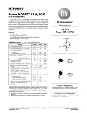
MTD2955V
Power MOSFET 12 A, 60 V
P−Channel DPAK
This Power MOSFET is designed to withstand high energy in the
avalanche and commutation modes. Designed for low voltage, high
speed switching applications in power supplies, converters and power
motor controls, these devices are particularly well suited for bridge
circuits where diode speed and commutating safe operating areas are
critical and offer additional safety margin against unexpected voltage
transients.
Features
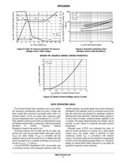
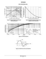
• Avalanche Energy Specified
• I
DSS
and V
DS(on)
Specified at Elevated Temperature
• Pb−Free Packages are Available
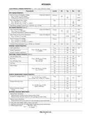
MAXIMUM RATINGS (T
C
= 25°C unless otherwise noted)
Rating Symbol Value Unit
Drain−to−Source Voltage V
DSS
60 Vdc
Drain−to−Gate Voltage (R
GS
= 1.0 M) V
DGR
60 Vdc
Gate−to−Source Voltage
− Continuous
− Non−repetitive (t
p
≤ 10 ms)
V
GS
V
GSM
± 20
± 25
Vdc
Vpk
Drain Current − Continuous
Drain Current − Continuous @ 100°C
Drain Current − Single Pulse (t
p
≤ 10 s)
I
D
I
D
I
DM
12
8.0
42
Adc
Apk
Total Power Dissipation
Derate above 25°C
Total Power Dissipation @ 25°C (Note 2)
P
D
60
0.4
2.1
Watts
W/°C
Watts
Operating and Storage Temperature
Range
T
J
, T
stg
−55 to
175
°C
Single Pulse Drain−to−Source Avalanche
Energy − Starting T
J
= 25°C
(V
DD
= 25 Vdc, V
GS
= 10 Vdc, Peak
I
L
= 12 Apk, L = 3.0 mH, R
G
= 25 )
E
AS
216 mJ
Thermal Resistance
− Junction to Case
− Junction to Ambient (Note 1)
− Junction to Ambient (Note 2)
R
JC
R
JA
R
JA
2.5
100
71.4
°C/W
Maximum Lead Temperature for Soldering
Purposes, 1/8″ from case for 10
seconds
T
L
260 °C
Maximum ratings are those values beyond which device damage can occur.
Maximum ratings applied to the device are individual stress limit values (not
normal operating conditions) and are not valid simultaneously. If these limits
are exceeded, device functional operation is not implied, damage may occur
and reliability may be affected.
1. When surface mounted to an FR4 board using the minimum recommended
pad size.
2. When surface mounted to an FR4 board using the 0.5 sq.in. pad size.
D
S
G
12 A, 60 V
R
DS(on)
= 185 m (Typ)
P−Channel
http://onsemi.com
DPAK−3
CASE 369C
STYLE 2
1
2
3
4
DPAK−3
CASE 369D
STYLE 2
1
2
3
4
See detailed ordering and shipping information in the
package dimensions section on page 7 of this data sheet.
ORDERING INFORMATION
See general marking information in the device marking
section on page 7 of this data sheet.
DEVICE MARKING INFORMATION