
下载
MRFE6VS25L
1
RF Device Data
NXP Semiconductors
RF Power LDMOS Transistor
High Ruggedness N--Channel
Enhancement--Mode Lateral MOSFET
RF power transistor designed for both narrowband and broadband ISM,
broadcast and aerospace applications operating at f requencies f rom 1.8 to
2000 MHz. This device is fabricated using NXP’s enhanced ruggedness
platform and is suitable for use in applications where high VSWRs are
encountered.
Typical Performance: V
DD
=50Vdc
Frequency
(MHz)
Signal Type
P
out
(W)
G
ps
(dB)
η
D
(%)
IMD
(dBc)
1.8--30
(1,3)
Two--Tone
(10 kHz spacing)
25 PEP 25.0 50.0 -- 2 8
30--512
(2,3)
Two--Tone
(200 kHz spacing)
25 PEP 17.3 32.0 -- 3 2
512
(4)
Pulse
(100 μsec, 20%
Duty Cycle)
25 Peak 25.9 74.0 —
512
(4)
CW 25 26.0 75.0 —
Load Mismatch/Ruggedness
Frequency
(MHz)
Signal Type VSWR
P
in
(W)
Test
Voltage
Result
30
(1)
CW
>65:1
at all Phase
Angles
0.11
(3 dB
Overdrive)
50 No Device
Degradation
512
(2)
CW 0.95
(3 dB
Overdrive)
512
(4)
Pulse
(100 μsec, 20%
Duty Cycle)
0.14 Peak
(3 dB
Overdrive)
512
(4)
CW 0.14
(3 dB
Overdrive)
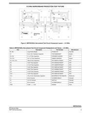
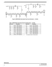
1. Measured in 1.8--30 MHz broadband reference circuit.
2. Measured in 30--512 MHz broadband reference circuit.
3. The values shown are the minimum measured performance numbers across the in-
dicated frequency range.
4. Measured in 512 MHz narrowband test circuit.
Features
• Wide operating frequency range
• Extreme ruggedness
• Unmatched, capable of very broadband operation
• Integrated stability enhancements
• Low thermal resistance
• Extended ESD protection circuit
Document Number: MRFE6VS25L
Rev. 1, 03/2017
NXP Semiconductors
Technical Data
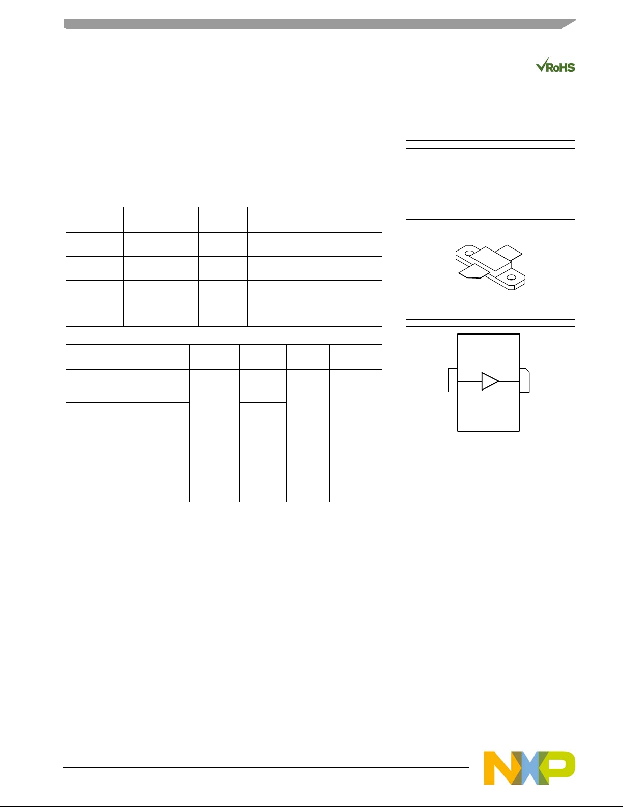
1.8--2000 MHz, 25 W, 50 V
WIDEBAND
RF POWER LDMOS TRANSISTOR
MRFE6VS25L
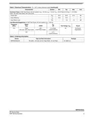
Note: The backside of the package is the
source terminal for the transistor.
NI--360H--2L
(Top View)
Drain
21
Figure 1. Pin Connections
Gate
© 2012, 2017 NXP B.V.