

下载
© Semiconductor Components Industries, LLC, 2015
January, 2015 − Rev. 10
1 Publication Order Number:
MJE18008/D
MJE18008, MJF18008
Switch-mode NPN Bipolar
Power Transistor
For Switching Power Supply Applications
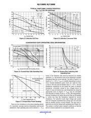
The MJE/MJF18008 have an applications specific state−of−the−art
die designed for use in 220 V line−operated switch−mode Power
supplies and electronic light ballasts.
Features
• Improved Efficiency Due to Low Base Drive Requirements:
♦ High and Flat DC Current Gain h
FE
♦
Fast Switching
♦ No Coil Required in Base Circuit for Turn−Off (No Current Tail)
• Tight Parametric Distributions are Consistent Lot−to−Lot
• Two Package Choices: Standard TO−220 or Isolated TO−220
• MJF18008, Case 221D, is UL Recognized at 3500 V
RMS
: File
#E69369
• These Devices are Pb−Free and are RoHS Compliant*
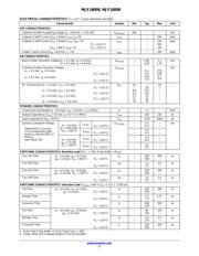
MAXIMUM RATINGS
Rating Symbol Value Unit
Collector−Emitter Sustaining Voltage V
CEO
450 Vdc
Collector−Base Breakdown Voltage V
CES
1000 Vdc
Emitter−Base Voltage V
EBO
9.0 Vdc
Collector Current − Continuous I
C
8.0 Adc
Collector Current − Peak (Note 1) I
CM
16 Adc
Base Current − Continuous I
B
4.0 Adc
Base Current − Peak (Note 1) I
BM
8.0 Adc
RMS Isolation Voltage (Note 2)
Test No. 1 Per Figure 22a
Test No. 1 Per Figure 22b
Test No. 1 Per Figure 22c
(for 1 sec, R.H. < 30%, T
A
= 25_C)
V
ISOL
MJF18008
4500
3500
1500
V
Total Device Dissipation @ T
C
= 25_C
MJE18008
MJF18008
Derate above 25°C MJE18008
MJF18008
P
D
125
45
1.0
0.36
W
W/_C
Operating and Storage Temperature T
J
, T
stg
−65 to 150
_C
THERMAL CHARACTERISTICS
Characteristics Symbol Max Unit
Thermal Resistance, Junction−to−Case
MJE18008
MJF18008
R
q
JC
1.0
2.78
_C/W
Thermal Resistance, Junction−to−Ambient
R
q
JA
62.5
_C/W
Maximum Lead Temperature for Soldering
Purposes 1/8″ from Case for 5 Seconds
T
L
260
_C
Stresses exceeding those listed in the Maximum Ratings table may damage the
device. If any of these limits are exceeded, device functionality should not be
assumed, damage may occur and reliability may be affected.
1. Pulse Test: Pulse Width = 5 ms, Duty Cycle ≤ 10%.
2. Proper strike and creepage distance must be provided.
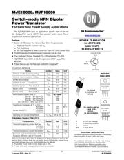
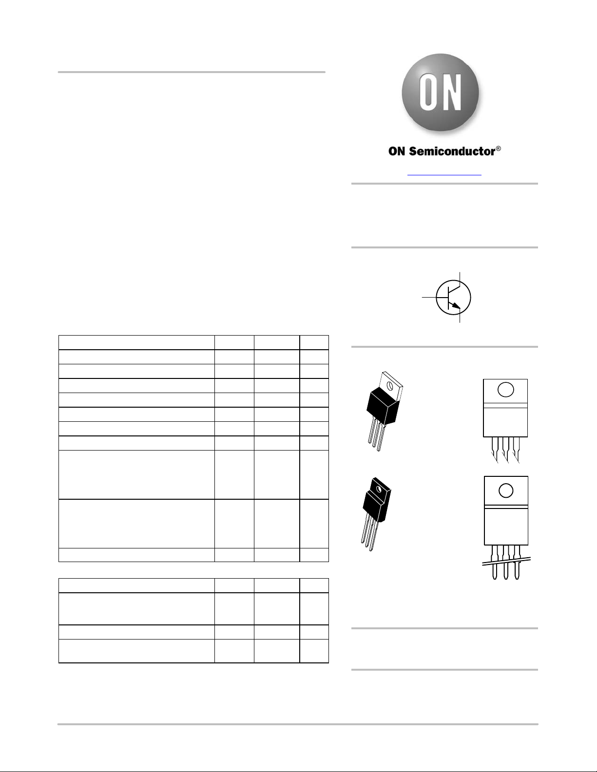
POWER TRANSISTOR
8.0 AMPERES
1000 VOLTS
45 and 125 WATTS
TO−220AB
CASE 221A−09
STYLE 1
1
www.onsemi.com
MARKING
DIAGRAMS
2
3
G = Pb−Free Package
A = Assembly Location
Y = Year
WW = Work Week
MJE18008G
AYWW
See detailed ordering and shipping information in the package
dimensions section on page 7 of this data sheet.
ORDERING INFORMATION
TO−220 FULLPACK
CASE 221D
STYLE 2
UL RECOGNIZED
3
1
2
MJF18008G
AYWW
*For additional information on our Pb−Free strategy
and soldering details, please download the
ON Semiconductor Soldering and Mounting
Techniques Reference Manual, SOLDERRM/D.
4
1
BASE
3
EMITTER
COLLECTOR
2,4