
下载
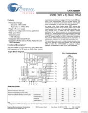
256K (32K x 8) Static RAM
CY7C1399BN
Cypress Semiconductor Corporation • 198 Champion Court • San Jose, CA 95134-1709 • 408-943-2600
Document #: 001-06490 Rev. *A Revised August 31, 2006
Features
• Temperature Ranges
— Industrial: –40°C to 85°C
— Automotive-A: –40°C to 85°C
• Single 3.3V power supply
• Ideal for low-voltage cache memory applications
• High speed: 12 ns
• Low active power
— 180 mW (max.)
• Low-power alpha immune 6T cell
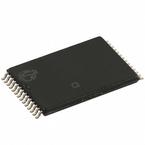
• Available in Pb-free and non Pb-free Plastic SOJ and
TSOP I packages
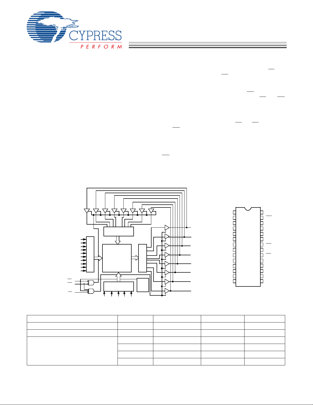
Functional Description
[1]
The CY7C1399BN is a high-performance 3.3V CMOS Static
RAM organized as 32,768 words by 8 bits. Easy memory
expansion is provided by an active LOW Chip Enable (CE
) and
active LOW Output Enable (OE
) and tri-state drivers. The
device has an automatic power-down feature, reducing the
power consumption by more than 95% when deselected.
An active LOW Write Enable signal (WE
) controls the
writing/reading operation of the memory. When CE
and WE
inputs are both LOW, data on the eight data input/output pins
(I/O
0
through I/O
7
) is written into the memory location
addressed by the address present on the address pins (A
0
through A
14
). Reading the device is accomplished by selecting
the device and enabling the outputs, CE
and OE active LOW,
while WE
remains inactive or HIGH. Under these conditions,
the contents of the location addressed by the information on
address pins is present on the eight data input/output pins.
The input/output pins remain in a high-impedance state unless
the chip is selected, outputs are enabled, and Write Enable
(WE
) is HIGH. The CY7C1399BN is available in 28-pin
standard 300-mil-wide SOJ and TSOP Type I packages.
Note:
1. For guidelines on SRAM system design, please refer to the ‘System Design Guidelines’ Cypress application note, available on the internet at www.cypress.com.
Selection Guide
-12 -15 -20
Maximum Access Time (ns) 12 15 20
Maximum Operating Current (mA) 55 50 45
Maximum CMOS Standby Current (µA) Commercial 500 500 500
Commercial (L) 50 50 50
Industrial 500 500
Automotive-A 500
L
og
i
c
Bl
oc
k
Di
agram
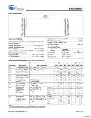
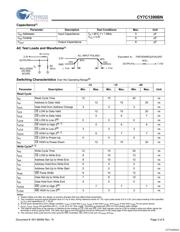
Pin Configurations
1
2
3
4
5
6
7
8
9
10
11
14
15
16
20
19
18
17
21
24
23
22
Top View
SOJ
12
13
25
28
27
26
GND
A
6
A
7
A
8
A
9
A
10
A
11
A
12
A
13
WE
V
CC
A
4
A
3
A
2
A
1
I/O
7
I/O
6
I/O
5
I/O
4
A
14
A
5
I/O
0
I/O
1
I/O
2
CE
OE
A
0
I/O
3
A
1
A
2
A
3
A
4
A
5
A
6
A
7
A
8
COLUMN
DECODER
ROW DECODER
SENSE AMPS
INPUT BUFFER
POWER
DOWN
WE
OE
I/O
0
CE
I/O
1
I/O
2
I/O
3
32K x 8
ARRAY
I/O
7
I/O
6
I/O
5
I/O
4
A
9
A
0
A
11
A
13
A
12
A
14
A
10
[+] Feedback