
下载
Semiconductor Components Industries, LLC, 2005
February, 2005 − Rev. 3
1 Publication Order Number:
BCW65ALT1/D
BCW65ALT1, BCW65CLT1
General Purpose Transistor
NPN Silicon
Features
• Pb−Free Package is Available
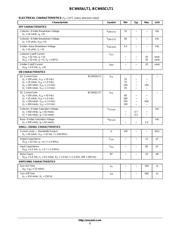
MAXIMUM RATINGS
Rating Symbol Value Unit
Collector−Emitter Voltage V
CEO
32 Vdc
Collector−Base Voltage V
CBO
60 Vdc
Emitter−Base Voltage V
EBO
5.0 Vdc
Collector Current − Continuous I
C
800 mAdc
Maximum ratings are those values beyond which device damage can occur.
Maximum ratings applied to the device are individual stress limit values (not
normal operating conditions) and are not valid simultaneously. If these limits
are exceeded, device functional operation is not implied, damage may occur
and reliability may be affected.
THERMAL CHARACTERISTICS
Characteristic Symbol Max Unit
Total Device Dissipation FR−5 Board
(Note 1), T
A
= 25°C
Derate above 25°C
P
D
225
1.8
mW
mW/°C
Thermal Resistance,
Junction−to−Ambient
R
JA
556 °C/W
Total Device Dissipation Alumina
Substrate, (Note 2) T
A
= 25°C
Derate above 25°C
P
D
300
2.4
mW
mW/°C
Thermal Resistance,
Junction−to−Ambient
R
JA
417 °C/W
Junction and Storage Temperature T
J
, T
stg
−55 to +150 °C
1. FR−5 = 1.0 0.75 0.062 in.
2. Alumina = 0.4 0.3 0.024 in 99.5% alumina.
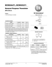
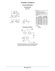
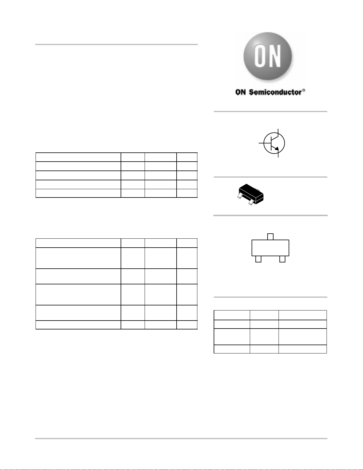
SOT−23
CASE 318
STYLE 6
http://onsemi.com
EA= Specific Device Code (BCW65ALT1)
EC= Specific Device Code (BCW65CLT1)
M = Date Code
MARKING DIAGRAM
1
2
3
Device Package Shipping
†
ORDERING INFORMATION
BCW65ALT1 SOT−23 3000 / Tape & Reel
BCW65ALT1G SOT−23
(Pb−Free)
3000 / Tape & Reel
†For information on tape and reel specifications,
including part orientation and tape sizes, please
refer to our Tape and Reel Packaging Specifications
Brochure, BRD8011/D.
Ex M
3000 / Tape & Reel
COLLECTOR
3
1
BASE
2
EMITTER
BCW65CLT1 SOT−23 3000 / Tape & Reel