
下载
BC817-16 / -25 / -40
Document number: DS11107 Rev. 18 - 2
1 of 4
www.diodes.com
April 2009
© Diodes Incorporated
BC817-16 / -25 / -40
NPN SURFACE MOUNT SMALL SIGNAL TRANSISTOR
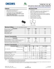
Features
• Ideally Suited for Automated Insertion
• Epitaxial Planar Die Construction
• For Switching, AF Driver and Amplifier Applications
• Complementary PNP Types Available (BC807)
• Lead, Halogen and Antimony Free, RoHS Compliant
• "Green" Device (Notes 3 and 4)
• Qualified to AEC-Q101 Standards for High Reliability
Mechanical Data
• Case: SOT-23
• Case Material: Molded Plastic, “Green” Molding Compound,
Note 4. UL Flammability Classification Rating 94V-0
• Moisture Sensitivity: Level 1 per J-STD-020D
• Terminals: Matte Tin Finish annealed over Alloy 42 leadframe
(Lead Free Plating) Solderable per MIL-STD-202, Method 208
• Pin Connections: See Diagram
• Marking Information: See Page 3
• Ordering Information: See Page 3
• Weight: 0.008 grams (approximate)
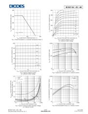
Maximum Ratings @T
A
= 25°C unless otherwise specified
Characteristic Symbol Value Unit
Collector-Emitter Voltage
V
CEO
45 V
Emitter-Base Voltage
V
EBO
5.0 V
Collector Current
I
C
800 mA
Peak Collector Current
I
CM
1000 mA
Peak Emitter Current
I
EM
1000 mA
Thermal Characteristics
Characteristic Symbol Value Unit
Power Dissipation at T
SB
= 50°C (Note 1) P
D
310 mW
Thermal Resistance, Junction to Substrate Backside (Note 1)
R
θ
SB
320 °C/W
Thermal Resistance, Junction to Ambient Air (Note 1)
R
θ
JA
403 °C/W
Operating and Storage Temperature Range
T
J
, T
STG
-65 to +150 °C
Electrical Characteristics @T
A
= 25°C unless otherwise specified
Characteristic (Note 2) Symbol Min Max Unit Test Condition
DC Current Gain
Current Gain Group -16
-25
-40
h
FE
100
160
250
250
400
600
—
V
CE
= 1.0V, I
C
= 100mA
Current Gain Group -16
-25
-40
60
100
170
—
—
—
—
V
CE
= 1.0V, I
C
= 300mA
Collector-Emitter Saturation Voltage
V
CE
(
SAT
)
— 0.7 V
I
C
= 500mA, I
B
= 50mA
Base-Emitter Voltage
V
BE
— 1.2 V
V
CE
= 1.0V, I
C
= 300mA
Collector-Emitter Cutoff Current
I
CES
—
100
5.0
nA
µA
V
CE
= 45V
V
CE
= 25V, T
j
= 150°C
Emitter-Base Cutoff Current
I
EBO
— 100 nA
V
EB
= 4.0V
Gain Bandwidth Product
f
T
100 — MHz
V
CE
= 5.0V, I
C
= 10mA,
f = 50MHz
Collector-Base Capacitance
C
CBO
— 12 pF
V
CB
= 10V, f = 1.0MHz
Notes: 1. Device mounted on Ceramic Substrate 0.7mm; 2.5cm
2
area.
2. Short duration pulse test used to minimize self-heating effect.
3. No purposefully added lead. Halogen and Antimony Free.
4. Product manufactured with Data Code V9 (week 33, 2008) and newer are built with Green Molding Compound. Product manufactured prior to Date Code
V9 are built with Non-Green Molding Compound and may contain Halogens or Sb
2
O
3
Fire Retardants.
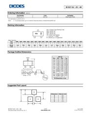
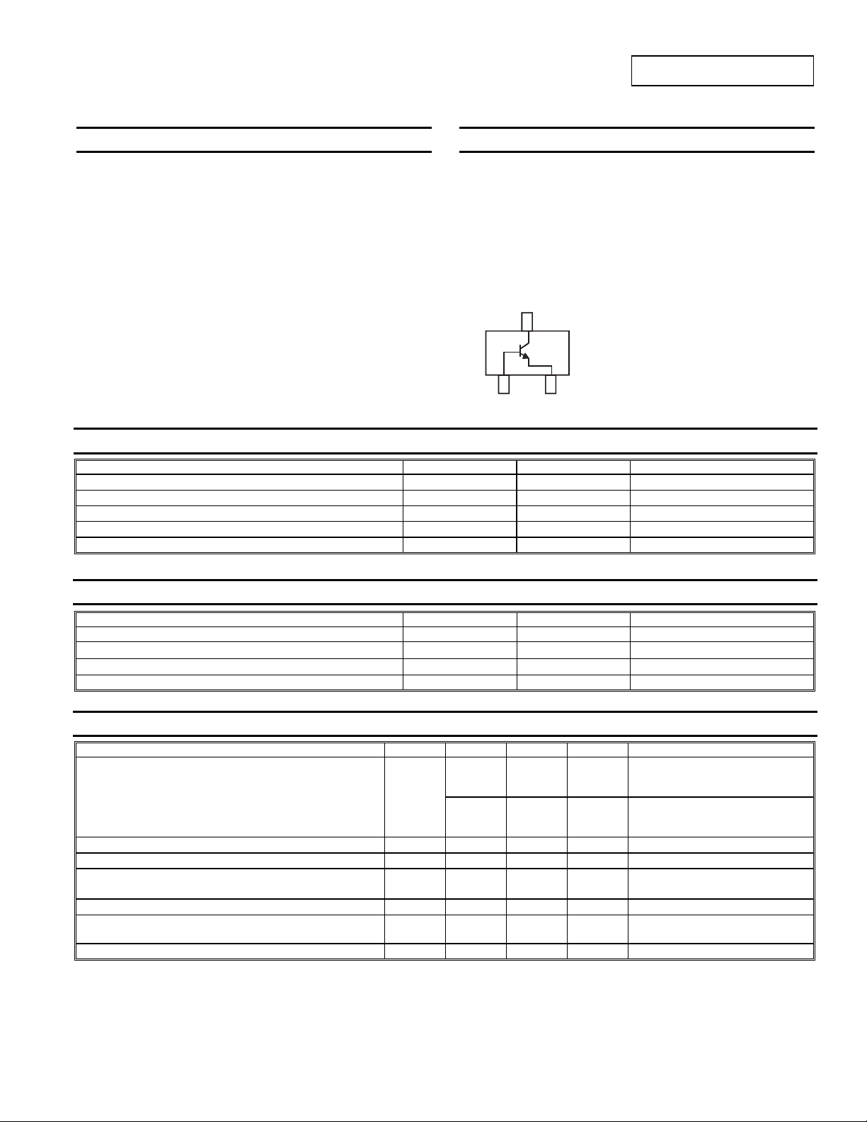
Top View
Device Schematic
E
B
C
Please click here to visit our online spice models database.
页面指南