
下载
LF to 2.7GHz Dual 60dB TruPwr Detector
PRELIMINARY TECHNICAL DATA
AD8364
Rev. PrC 1/20/2005
Information furnished by Analog Devices is believed to be accurate and reliable.
However, no responsibility is assumed by Analog Devices for its use, nor for any
infringements of patents or other rights of third parties that may result from its use.
Specifications subject to change without notice. No license is granted by implication
or otherwise under any patent or patent rights of Analog Devices. Trademarks and
registered trademarks are the property of their respective companies.
One Technology Way, P.O. Box 9106, Norwood, MA 02062-9106, U.S.A.
Tel: 781.329.4700 www.analog.com
Fax: 781.326.8703 © 2005 Analog Devices, Inc. All rights reserved.
FEATURES
RMS Measurement of High Crest-Factor Signals
Dual Channel and Difference Outputs ports
Integrated accurately scaled Temperature Sensor
Wide Dynamic Range ±1 dB over 60 dB @2.2 GHz
±0.5 dB Temperature-Stable Linear-in-dB Response
Low log conformance ripple
+5V Operation at 70 mA, –40°C to +85°C
Small footprint 5x5 mm LFCSP Package
APPLICATIONS
Wireless Infrastructure Power Amplifier Linearization/Control
Antenna VSWR Monitor Devices
Gain Control and Measurement
Transmitter Signal Strength Indication (TSSI)
Dual-Channel Wireless Infrastructure Radios
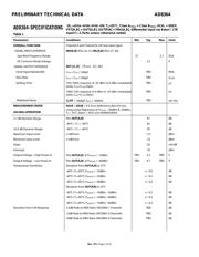
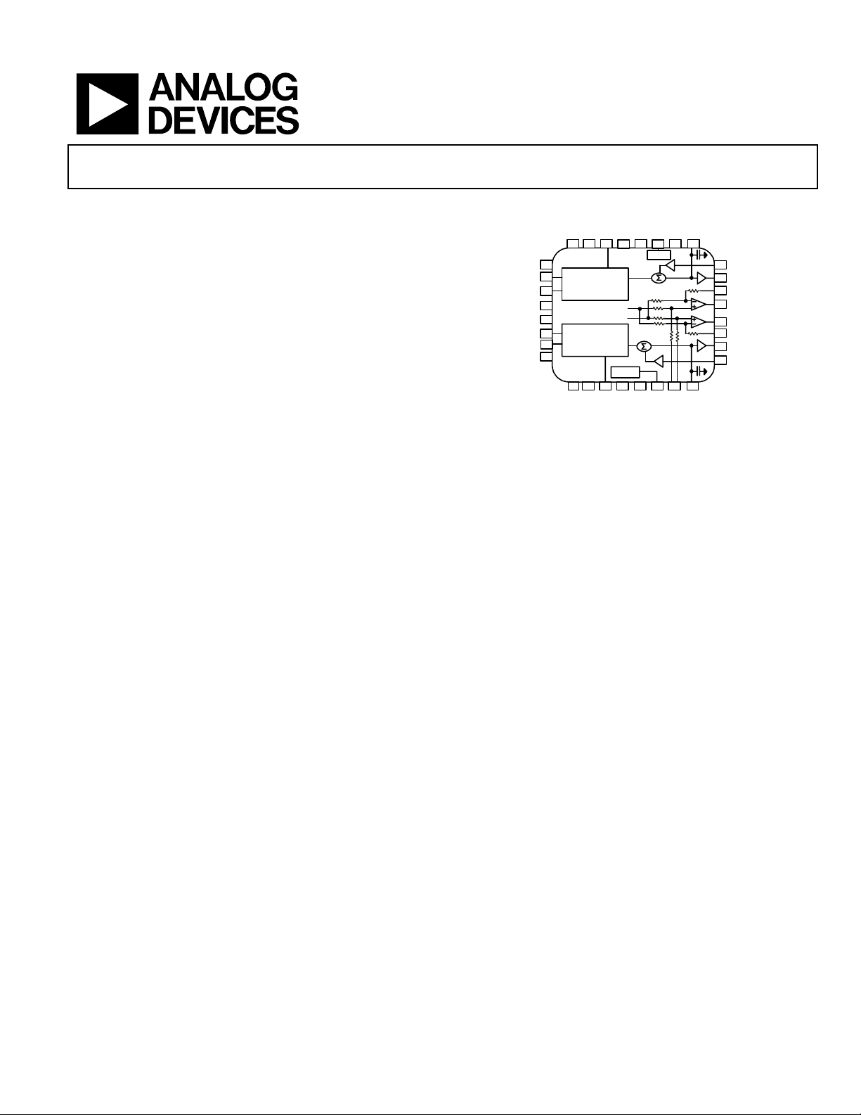
FUNCTIONAL BLOCK DIAGRAM
DECA
INLA
COMR
PWD
N
INLB
INHB
DECB
OUTB
VSTB
FBKB
OUTN
OUTP
FBKA
OUTA
VSTA
INHA
CHPA
VPSA
COMA
VPSR ACMB TEMPACMA CLPA
CHPB
VPSB
COMB ADJB ADJA
VREF VLVL CLPB
TEMP
Channel A
TruPwr™
V2I
BIAS
V2I
OUTA
OUTB
25
1 2 3 4 5 6
13
15
14
16
12
11
10
9
87
24 23 22 21 20 19 1718
Channel B
TruPwr™
2
2
2
2
3
3
3
6
7
8
9
0
1
2
Figure 1. Functional Block Diagram
GENERAL DESCRIPTION
The AD8364 is a true RMS responding dual channel RF power
measurement subsystem for the precise measurement and control
of signal power. The flexibility of the AD8364 allows
communications systems and instrumentation, such as RF power
amplifiers and radio transceiver AGC circuits, to be monitored and
controlled with ease. Operating on a single 5V supply, each
channel is fully specified for operation up to 2.7GHz, over a
dynamic range of 60dB. The AD8364 provides accurately scaled,
independent, RMS outputs of both RF measurement channels. A
useful measurement difference between the two channels is also
made available. On chip channel matching makes the RMS
difference output extremely stable with temperature and process
variations. The device also includes a useful temperature sensor
with an accurately scaled voltage proportional to temperature,
specified over the device operating temperature range. The
AD8364 can be used with input signals having RMS values from -
55dBm to +5dBm, Re: 50Ω and large crest factors with no accuracy
degradation.
Integrated in the AD8364 are two well-matched AD8362 channels
(see AD8362 data sheet for more info). Enhancements include
improved temperature performance and reduced log-conformance
ripple versus the AD8362. On chip wide bandwidth op-amps are
connected to accommodate flexible configurations that support
many system solutions.
The device can easily be configured to provide three RMS
measurements simultaneously. Linear-in-dB RMS measurements are
supplied at OUTA and OUTB, with conveniently scaled slope of
50mV/dB. The RMS difference between OUTA and OUTB is
available differentially or single-ended at OUTP and OUTN. An
optional voltage applied to VLVL provides a common mode
reference level to offset OUTP and OUTN above ground.
Each channel of the AD8364 can independently be used to control
separate gain control feedback loops using VSTA and VSTB. The
difference outputs also provide feedback control while providing
improved temperature stability through matched channels.
Flexibility exists to use either channel as a reference while the other
channel is slaved through a feedback loop. RF power amplifier
control, VSWR measurements, and transceiver AGC circuits benefit
from this feature. In control modes, the opposite polarities of the
OUTP and OUTN outputs allow proportional or complementary
gain-control functions, eliminating the need for a board-level sign-
inverting amplifier. Feedback pins FBKA and FBKB allow custom
loop regulation in special control system applications and log-slope
adjust flexibility. When one channel is slaved off the other,
controlling the voltage at VLVL will adjust the slaved channel’s RMS
value, if a power level offset is desired.
The AD8364 is supplied in a 32-lead 5x5mm LFCSP package, for the
operating temperature of –40
o
C to +85
o
C.