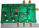
This Evaluation Module (EVM) facilitates the experimental testing of the Texas Instruments SN65LVDS19 Repeater/Translator silicon device. This device accepts CML, PECL or LVDS input levels and Translates them to LVDS output levels as defined by TIA/EIA-644-A standard at 12 mA’s drive current.
The device operates at rates to 2.0Gbps or clock rates to 1.0 GHz at either 3.3 V or 2.5 V supply operation, with less than 23 ps of total jitter. The device output can be disabled to the high impedance state by applying a logic High level to the EN bar pin.
This device also provides a voltage reference output (Vbb) of typically 1.35 V below Vcc for use in receiving single-ended PECL input signals. A Gain Control input (GC), is provided for selecting output amplitudes from 300mV to 860mV on the /Q output.