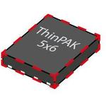
The new CoolMOS™ ThinPAK 5x6 is a leadless SMD package especially designed for high voltage MOSFETs. This new package has a very small footprint of 5x6mm 2 and a very low profile with only 1mm height.
This significantly smaller package size in combination with its benchmark low parasitics inductances can be used as a new and effective way to decrease system solution size in power- density driven designs. The ThinPAK 5x6 package is characterized by a very low source inductance 1.6nH, as well as a similar thermal performance as DPAK.
The package hence enables faster and thus more efficient switching of power MOSFETs and is easier to handle in terms of switching behavior and EMI.