sales@aipcba.com
CN
电子元器件采购 > ON Semiconductor >

FXWA9306L8X 库存 & 价格

FXWA9306L8X
显示的图像仅供参考,应从产品数据表中获得准确的规格。
FXWA9306L8X ON Semiconductor
ON Semiconductor
  • 制造商:
    ON Semiconductor
  • 制造商型号#:
    FXWA9306L8X
  • 百芯编号#:
    CM56361382
  • 价格(CNY): ¥ 5.13
  • 百芯库存:
    1,206
  • 可供应量:
    622 个在库
    此为供应商库存,需要与销售确认
  • 产品描述:
    Voltage Level Translator 8Pin MicroPak T/R
  • 文档: 符合 RoHS 标准 3D模型
FXWA9306L8X 购买 FXWA9306L8X 库存和价格更新于 2024-05-17 03:50:22
  • 刷新
    器件型号: FXWA9306L8X
    百芯编号: CM56361382
    制造商: ON Semiconductor
    价格 ¥5.13
    总计: 1,828
    MOQ: 1
    库存地点: 香港
    发货日期: 2024/05/22 (预期 )
  • 购买
    *由于库存数量、价格不断波动,请 联系我们 获取型号最新价格和库存。

    元器件库存查询

    库存查询
    百芯库存涵盖200,000个元器件
    欺诈预防提醒
    近日,我们发现不法分子冒充百芯智造进行诈骗或试图低价销售假冒和故障元器件。
    百芯智造在2021年建立了一个 元器件检测实验室 ,旨在提供有质量保证的组件。
    我们强烈建议客户选择可靠的元器件供应商。
    请注意,唯一电子邮件后缀是 aipcba.com
    FXWA9306L8X 规格 显示相似产品 (99+)
    类型
    描述
    选择
    制造商
    ON Semiconductor
    安装方式
    Surface Mount
    3D模型
     3D模型
    引脚数
    8 Pin
    封装
    UQFN-8
    电路数
    1 Circuit
    通道数
    2 Channel
    针脚数
    8 Position
    输入数
    2 Input
    工作温度(Max)
    85 ℃
    工作温度(Min)
    -40 ℃
    电源电压(Max)
    5.5 V
    电源电压(Min)
    1 V
    显示相似产品
    FXWA9306L8X 数据规格书
    FXWA9306L8X 数据手册Datasheet
    11 Pages, 391 KB
    2017/09/20
    查看
    FXWA9306L8X 其它数据手册Datasheet
    10 Pages, 789 KB
    查看
    FXWA9306L8X 产品设计图
    2 Pages, 28 KB
    2016/08/11
    查看
    尺寸 & 包装
    类型
    描述
    长度
    1.6 mm
    宽度
    1.6 mm
    高度
    0.5 mm
    工作温度
    -40℃ ~ 85℃ (TA)
    产品生命周期
    Active
    包装方式
    Tape & Reel (TR)
    符合标准
    类型
    描述
    RoHS标准
    RoHS Compliant
    含铅标准
    Lead Free
    出口分类
    类型
    描述
    ECCN代码
    EAR99
    产品概述
    • The FXWA9306 is a dual, bi-directional, IC-bus and SMBus, voltage-level translator with an enable (OE) input that is operational from 1.0V to 3.6V (V) without requiring a direction pin. C-bus systems, the pull-up resistors are required to provide the logic HIGH levels on the translator"s bus. The FXWA9306 has a standard open-drain configuration of the IC bus. The size of these pull-up resistors depends on the system, but each side of the translator must have a pull-up resistor. The device is designed to work with Standard-Mode, Fast-Mode, and Fast Mode Plus IC-bus devices in addition to SMBus devices. The maximum frequency is dependent on the RC time constant, but generally supports up to 2MHz. All channels have the same electrical characteristics and there is a minimum deviation from one output to another in voltage or propagation delay. This is a benefit over discrete transistor voltage translation solutions, since the fabrication of the switch is symmetrical. The translator provides excellent ESD protection to lower voltage devices and at the same time protects less-ESD resistant devices.
    • Features
    • ---
    •  |
    • 2-Bit Bi-Directional Translator for SDA and SCL Lines in Mixed-Mode I2C-Bus Applications
    • Standard-Mode, Fast-Mode, and Fast-Mode-Plus I2C-Bus and SMBus Compatible
    • Less than 1.5ns Maximum Propagation Delay to Accommodate Standard-Mode and Fast-Mode I2C-Bus Devices and Multiple Masters
    • Allows Voltage Level Translation Between:
    • 1.0V VCCA and 1.8V, 2.5V, 3.3V, or 5V VCCB
    • 1.2V VCCA and 1.8V, 2.5V, 3.3V, or 5V VCCB
    • 1.8V VCCA and 3.3V or 5V VCCB
    • 2.5V VCCA and 5V VCCB
    • 3.3V VCCA and 5V VCCB
    • Supports I2C Clock Stretching and Multi-Master
    • Provides Bi-Directional Voltage Translation without Direction Pin
    • Low 3.5Ω On-State Connection Between Input and Output Ports; Provides Less Signal Distortion
    • Open-Drain I2C-Bus I/O Ports (A0, A1, B0, and B1)
    • 5V-Tolerant I2C-Bus I/O Ports to Support Mixed-Mode Signal Operation
    • Lock-Up-Free Operation
    • High-Impedance A0, A1, B0, and B1 Pins for OE = LOW
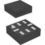
    • Packaged in 8-Terminal Leadless MicroPak™ (1.6mm x 1.6mm)
    • Flow-Through Pinout for Simpler Printed-Circuit Board Trace Routing
    • 4kV HBM ESD (per JESD22-A114)
    • ESD Protection Exceeds:
    • 1KV CDM (per JESD22-C101)
    • 8kV HBM ESD (Pin to Pin, B Port)

    百芯智造认证

    百芯智造承诺产品质量和安全通过ISO 9001、ISO 13485、ISO 45001、UL、RoHS、CQC 和 REACH 认证
    查看我们的认证 >
    订购详情及相关信息
    •  此处条款仅供参考,实际条款以销售报价为准。
      - 订购时请确认产品规格。
      - MOQ 是指购买每个零件所需的最小起订量。
      - 如果您有特殊的订购说明,请在订购页面注明。
      - 装运前会进行检验 (PSI)。
      - 您可以随时给我们发邮件查询订单状态。
      - 包裹发货后无法取消订单。
    • - 提前电汇(银行转账),也可选择PayPal。
      - 仅限现金转账。(不接受支票和账单转账。)
      - 客户负责支付所有可能的费用,包括销售税、增值税和海关费用等。
      - 如果您需要详细的发票或税号,请给我们发送电子邮件。
    • - 可选择顺丰或跑腿。
      - 您可以选择是通过您的运费帐户收取运费还是由我们收取。
      - 偏远地区请提前与物流公司确认。
      (在这些地区送货可能会收取额外费用(35-50 美元)。)
      - 交货日期:通常为 2 到 7 个工作日。
      - 您的订单发货后将发送跟踪号。
    • - 由百芯智造仓库仔细检查和包装
      - 真空包装
      - 防静电包装
      - 防震泡沫
    • - 收入质量控制 (IQC),800多家合格经销商。
      - 500m² 高级元器件检测实验室、假冒检测、RoHS 合规性等
      - 2000㎡数码元器件仓库,恒温恒湿
      - 开盖检查
      - X-Ray检查
      - XRF检查
      - 电气测试
      - 外观检测
    • - 不合格和假冒检测
      - 故障分析
      - 电气测试
      - 生命周期和可靠性测试
      -百芯2021年成立元器件检测实验室
      了解更多 >

    电子元件供应服务

    立即查看
    SN:H1.01457LO94590V11Q0QC0S1
    在线联系我们
    黄经理 - 百芯智造销售经理在线,5 分钟前
    您的邮箱 *
    消息 *
    发送