The AD5689R _nano_DAC+™ is a low power, dual, 16-bit buffered voltage output digital-to-analog converter (DAC). The device includes a 2.5 V, 2 ppm/°C internal reference (enabled by default) and a gain select pin giving a full-scale output of 2.5 V (gain = 1) or 5 V (gain = 2). The device operates from a single 2.7 V to 5.5 V supply, is guaranteed monotonic by design, and exhibits less than 0.1% FSR gain error and 1.5 mV offset error performance. The device is available in a 3 mm × 3 mm LFCSP and a TSSOP package.
The AD5689R also incorporates a power-on reset circuit and a RSTSEL pin that ensures that the DAC outputs power up to zero scale or midscale and remain there until a valid write takes place. The part contains a per channel power-down feature that reduces the current consumption of the device to 4 μA at 3 V while in power-down mode.
The AD5689R uses a versatile serial peripheral interface (SPI) that operates at clock rates up to 50 MHz. and contains a VLOGIC pin that is intended for 1.8 V/3 V/5 V logic.
**Product Highlights**
1. High Relative Accuracy (INL).
AD5689R (16-bit): ±2 LSB maximum
2. Low Drift 2.5 V On-Chip Reference.
2 ppm/°C typical temperature coefficient
5 ppm/°C maximum temperature coefficient
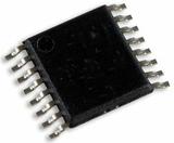
3. Two Package Options.
3 mm × 3 mm, 16-lead LFCSP
16-lead TSSOP
**Applications**
Optical transceivers
Base station power amplifiers
Process control (PLC I/O cards)
Industrial automation
Data acquisition systems
### Features and Benefits
High relative accuracy (INL): ±2 LSB maximum at 16 bits
Low drift 2.5 V reference: 2 ppm/°C typical
Tiny package: 3 mm × 3 mm, 16-lead LFCSP
TUE: ±0.1% of FSR maximum
Offset error: ±1.5 mV maximum
Gain error: ±0.1% of FSR maximum
High drive capability: 20 mA, 0.5 V from supply rails
See data sheet for additional features
**AD5689R-EP supports defense and aerospace applications (AQEC standard)**