
下载

1. General description
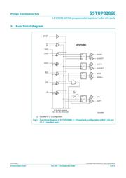
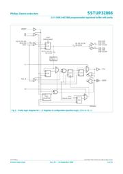
The SSTUP32866 is a 1.8 V configurable register specifically designed for use on DDR2
memory modules requiring a parity checking function. It is defined in accordance with the
JEDEC standard for the SSTUA32866 and SSTUB32866 registered buffers. The register
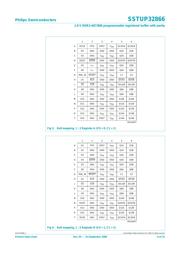
is configurable (using configuration pins C0 and C1) to two topologies: 25-bit 1 : 1 or
14-bit 1 : 2, and in the latter configuration can be designated as Register A or Register B
on the DIMM. It offers added features over the JEDEC standard register in that it can be
configured for high or normal output drive strength, as well as for operation to 667 MT/s or
800 MT/s, simply by tying two input pins HIGH or LOW as needed.
The SSTUP32866 accepts a parity bit from the memory controller on its parity bit
(PAR_IN) input, compares it with the data received on the DIMM-independent D-inputs
and indicates whether a parity error has occurred on its open-drain QERR pin
(active LOW). The convention is even parity, that is, valid parity is defined as an even
number of ones across the DIMM-independent data inputs combined with the parity input
bit.
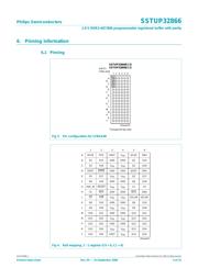
The SSTUP32866 is packaged in a 96-ball, 6 × 16 grid, 0.8 mm ball pitch LFBGA
package (13.5 mm × 5.5 mm).
2. Features
n Configurable register supporting DDR2 up to 667 MT/s or 800 MT/s Registered DIMM
applications
n Configurable to 25-bit 1 : 1 mode or 14-bit 1 : 2 mode
n Programmable for normal or high output drive
n Controlled multi-impedance output drivers enable optimal signal integrity and speed
n Programmable for 667 MT/s or 800 MT/s speed
n Excellent propagation delay performance
n Supports up to 450 MHz clock frequency of operation
n Optimized pinout for high-density DDR2 module design
n Chip-selects minimize power consumption by gating data outputs from changing state
n Supports SSTL_18 data inputs
n Checks parity on the DIMM-independent data inputs
n Partial parity output and input allows cascading of two SSTUP32866s for correct parity
error processing
n Differential clock (CK and CK) inputs
n Supports LVCMOS switching levels on the control and RESET inputs
n Single 1.8 V supply operation (1.7 V to 2.0 V)
SSTUP32866
1.8 V 25-bit 1 : 1 or 14-bit 1 : 2 configurable registered buffer
with parity and programmable output for DDR2-800 RDIMMs
Rev. 02 — 14 September 2006 Product data sheet
页面指南