


下载
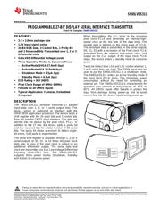
Application
Processor
with CMOS
Video Interface
LVDS301
or
LVDS311
DATA
CLK
or
LVDS302
LVDS314
LCD
SN65LVDS311
www.ti.com
SLLSE31B –MAY 2010–REVISED MARCH 2013
PROGRAMMABLE 27-BIT DISPLAY SERIAL INTERFACE TRANSMITTER
Check for Samples: SN65LVDS311
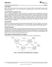
When transmitting, the PLL locks to the incoming
1
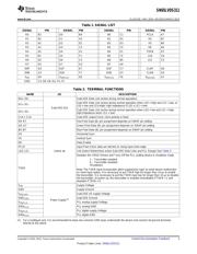
FEATURES
pixel clock PCLK and generates an internal high-
• 2.8 × 2.8mm package size
speed clock at the line rate of the data lines. The
• 1.8V input signal swing
parallel data is latched on the rising edge of PCLK.
The serialized data is presented on the serial outputs
• 24-Bit RGB Data, 3 Control Bits, 1 Parity Bit
D0, D1, D2 with a recreation of the Pixel clock PCLK
and 2 Reserved Bits Transmitted over 1, 2 or 3
generated from the internal high-speed clock and
Differential Lines
output on the CLK output. If the input clock PCLK
• SubLVDS Differential Voltage Levels
stops, the device enters a standby mode to conserve
• Three Operating Modes to Conserve Power
power.
– Active-Mode QVGA 17.4mW (typ)
Two Link-Select lines LS0 and LS1 control whether 1,
2 or 3 serial links are used. The TXEN input may be
– Active-Mode VGA 28.8mW (typ)
used to put the SN65LVDS311 in a shutdown mode.
– Shutdown Mode ≈ 0.5μA (typ)
The SN65LVDS311 enters an active Standby mode if
– Standby Mode ≈ 0.5μA (typ)
the input clock PCLK stops. This minimizes power
• ESD Rating > 3kV (HBM)
consumption without the need for controlling an
external pin. The SN65LVDS311 is characterized for
• Pixel Clock Range of 4MHz–65MHz
operation over ambient air temperatures of -40°C to
• Failsafe on all CMOS Inputs
85°C. All CMOS inputs offer failsafe to protect the
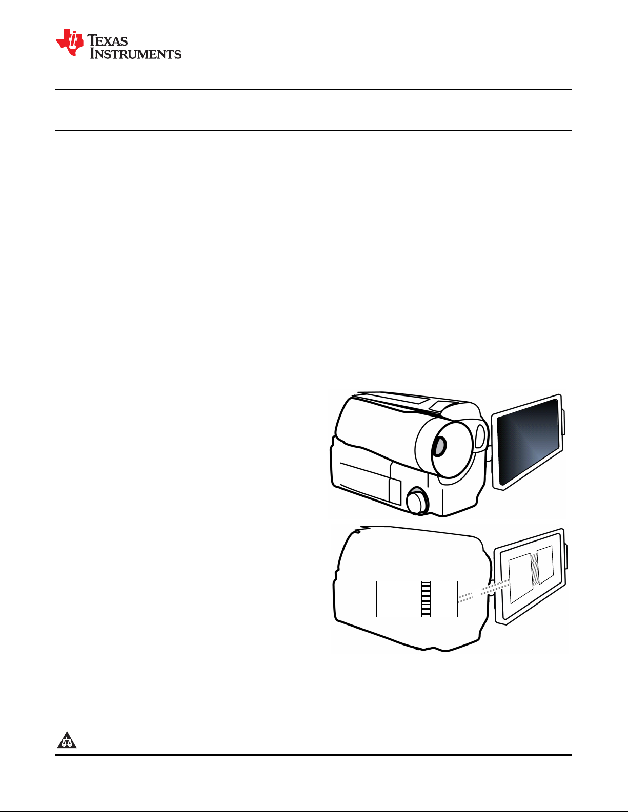
• Typical Application: Cameras, Embedded
input from damage during power-up and to avoid
Computers current flow into the device inputs during power-up.
DESCRIPTION
The SN65LVDS311 serializer transmits 27 parallel
input data over 1, 2, or 3 serial output links. The
device pinout is optimized to interface with the
OMAP3630 application processor. The device loads a
shift register with the 24 pixel bits and 3 control bits
from the parallel CMOS input interface. The data are
latched into the device by the pixel clock, PCLK. In
addition to the 27 bits, the device adds a parity bit
and two reserved bits for a total number of 30 serial
bits. The parity bit allows a receiver to detect single-
bit errors. Odd parity is implemented.
The serial shift register is uploaded through 1, 2, or 3
serial outputs at 30, 15, or 10 times the pixel clock
data rate. A copy of the pixel clock is output on an
additional differential output. The serial data and
clock are transmitted via Sub Low-Voltage Differential
Signaling (SubLVDS) lines. The SN65LVDS311
supports three power modes (Shutdown, Standby
and Active) to conserve power.
1
Please be aware that an important notice concerning availability, standard warranty, and use in critical applications of
Texas Instruments semiconductor products and disclaimers thereto appears at the end of this data sheet.
PRODUCTION DATA information is current as of publication date.
Copyright © 2010–2013, Texas Instruments Incorporated
Products conform to specifications per the terms of the Texas
Instruments standard warranty. Production processing does not
necessarily include testing of all parameters.
页面指南