
Rev. 1.1 8/12 Copyright © 2012 by Silicon Laboratories Si5356A
Si5356A
I
2
C PROGRAMMABLE, ANY-FREQUENCY 1–200 MHZ,
QUAD FREQUENCY 8-OUTPUT CLOCK GENERATOR
Features
Applications
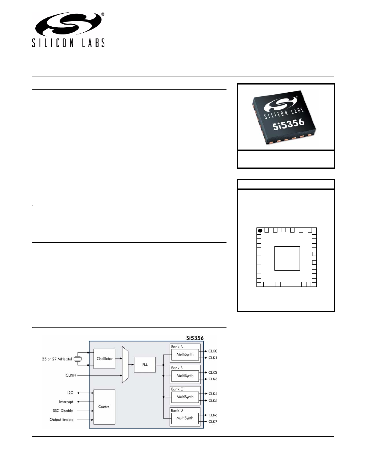
Description
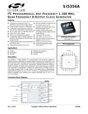
The Si5356 is a highly flexible, I
2
C programmable clock generator capable of
synthesizing four completely non-integer related frequencies up to 200 MHz. The
device has four banks of outputs with each bank supporting two CMOS outputs at
the same frequency. Using Silicon Laboratories' patented MultiSynth fractional
divider technology, all outputs are guaranteed to have 0 ppm frequency synthesis
error regardless of configuration, enabling the replacement of multiple clock ICs
and crystal oscillators with a single device. Each output bank is independently
configurable to support 1.8, 2.5, or 3.3 V. The device is programmable via an I
2
C/
SMBus-compatible serial interface and supports operation from a 1.8, 2.5, or
3.3 V core supply.
Functional Block Diagram
Generates any frequency from 1 to
200 MHz on each of the 4 output banks
Programmable frequency configuration
Guaranteed 0 ppm frequency synthesis
error for any combination of frequencies
25 or 27 MHz xtal or 5–200 MHz input clk
Eight CMOS clock outputs
Easy to use programming software
Configurable “triple A” spread spectrum:
any clock, any frequency, and with any
spread amount
Programmable output phase adjustment
with <20 ps error
Interrupt pin indicates LOS or LOL
OEB pin disables all outputs or per
bank OEB control via I
2
C
Low jitter: 50 ps pk-pk (typ), 75 ps
pk-pk period jitter (max)
Excellent PSRR performance
eliminates need for external power
supply filtering
Low power: 45 mA (core)
Core VDD: 1.8, 2.5, or 3.3 V
Separate VDDO for each bank of
outputs: 1.8, 2.5, or 3.3 V
Small size: 4x4 mm 24-QFN
Industrial temperature range:
–40 to +85 °C
Printers
Audio/video
DSLAM
Storage area networks
Switches/routers
Servers
Ordering Information:
See page 23.
Pin Assignments
XA
CLK5
CLK4
VDDOC
VDDOB
CLK3
CLK2
VDD
VDD
P2
CLK6
CLK7
LOS
P3
VDDOA
CLK1
CLK0
GND
VDDOD
GND
GND
XB
P1
CLKIN
P4
P5
Top View
1
6
5
4
3
2
712111098
18
13
14
15
16
17
24 1920212223
XA
CLK5
CLK4
VDDOC
VDDOB
CLK3
CLK2
VDD
VDD
SCL
CLK6
CLK7
INTR
SDA
VDDOA
CLK1
CLK0
GND
VDDOD
GND
GND
XB
I2C_LSB
CLKIN
SSC_DIS
OEB
Top View
1
6
5
4
3
2
712111098
18
13
14
15
16
17
24 1920212223