

Rev. 1.6 12/15 Copyright © 2015 by Silicon Laboratories Si5338
Si5338
I
2
C-PROGRAMMABLE ANY-FREQUENCY, ANY-OUTPUT
Q
UAD CLOCK GENERATOR
Features
Applications
Description
The Si5338 is a high-performance, low-jitter clock generator capable of
synthesizing any frequency on each of the device's four output drivers. This timing
IC is capable of replacing up to four different frequency crystal oscillators or
operating as a frequency translator. Using its patented MultiSynth™ technology,
the Si5338 allows generation of four independent clocks with 0 ppm precision.
Each output clock is independently configurable to support various signal formats
and supply voltages. The Si5338 provides low-jitter frequency synthesis in a
space-saving 4 x 4 mm QFN package. The device is programmable via an I
2
C/
SMBus-compatible serial interface and supports operation from a 1.8, 2.5, or
3.3 V core supply. I
2
C device programming is made easy with the ClockBuilder™
Desktop software available at www.silabs.com/ClockBuilder. Measuring PCIe
clock jitter is quick and easy with the Silicon Labs PCIe Clock Jitter Tool.
Download it for free at www.silabs.com/pcie-learningcenter.
Low power MultiSynth™ technology
enables independent, any-frequency
synthesis on four differential output
drivers
PCIe Gen 1/2/3/4 Common Clock and
Gen 3 SRNS compliant
Highly-configurable output drivers with
up to four differential outputs, eight
single-ended clock outputs, or a
combination of both
Low phase jitter of 0.7 ps RMS typ
High precision synthesis allows true
zero ppm frequency accuracy on all
outputs
Flexible input reference:
External crystal: 8 to 30 MHz
CMOS input: 5 to 200 MHz
SSTL/HSTL input: 5 to 350 MHz
Differential input: 5 to 710 MHz
Independently configurable outputs
support any frequency or format:
LVPECL/LVDS: 0.16 to 710 MHz
HCSL: 0.16 to 250 MHz
CMOS: 0.16 to 200 MHz
SSTL/HSTL: 0.16 to 350 MHz
Independent output voltage per driver:
1.5, 1.8, 2.5, or 3.3 V
Single supply core with excellent
PSRR: 1.8, 2.5, 3.3 V
Independent frequency increment/
decrement feature enables
glitchless frequency adjustments in
1 ppm steps
Independent phase adjustment on
each of the output drivers with an
accuracy of <20 ps steps
Highly configurable spread
spectrum (SSC) on any output:
Any frequency from 5 to 350 MHz
Any spread from 0.5 to 5.0%
Any modulation rate from 33 to
63 kHz
External feedback mode allows
zero-delay mode
Loss of lock and loss of signal
alarms
I
2
C/SMBus compatible interface
Easy to use programming software
Small size: 4 x 4 mm, 24-QFN
Low power: 45 mA core supply typ
Wide temperature range: –40 to
+85 °C
Ethernet switch/router
PCIe Gen1/2/3/4
Broadcast video/audio timing
Processor and FPGA clocking
Any-frequency clock conversion
MSAN/DSLAM/PON
Fibre Channel, SAN
Telecom line cards
1 GbE and 10 GbE
Ordering Information:
See page 42.
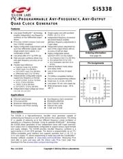
Pin Assignments
IN1
CLK2B
CLK2A
VDDO2
VDDO1
CLK1B
CLK1A
VDD
VDD
SCL
CLK3A
CLK3B
INTR
SDA
VDDO0
CLK0B
CLK0A
RSVD_GND
VDDO3
GND
GND
Pad
5
4
3
2
1
6 13
10
987
IN2
IN3
IN4
IN5
IN6
Top View
11
12
15
14
16
17
18
192021
222324
页面指南