

下载

2001 Microchip Technology Inc. DS39028E-page 1
PIC18CXXX
This document includes the
programming specifications for the
following devices:
1.0 PROGRAMMING THE
PIC18CXXX
The PIC18CXXX can be programmed using a serial
method while in users’ system, allowing increased
design flexibility. This programming specification
applies to PIC18CXXX devices in all package types.
1.1 Hardware Requirements
The PIC18CXXX requires two programmable power
supplies, one for V
DD and one for VPP. Both supplies
should have a minimum resolution of 0.25V.
1.2 Programming Mode
The Programming mode for the PIC18CXXX allows
programming of user program memory (except for the
PIC18C601/801 ROMless devices), special locations
used for ID, and the configuration words for the
PIC18CXXX.
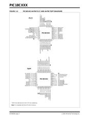
Pin Diagrams
The pin diagrams for the PIC18CXX2 family are shown
below in Figure 1-1 through Figure 1-3. Pin diagrams for
the PIC18CXX8 family are provided in Figure 1-4
through Figure 1-7. Pin diagrams for the PIC18C601/801
family are provided in Figure 1-8 through Figure 1-11.
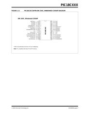
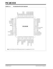
FIGURE 1-1: PIC18CXX2 FAMILY
PIN DIAGRAM
• PIC18C242 • PIC18C601
• PIC18C252 • PIC18C801
• PIC18C442 • PIC18C658
• PIC18C452 • PIC18C858
RB7
RB6
RB5
RB4
RB3/CCP2
*
RB2/INT2
RB1/INT1
RB0/INT0
V
DD
VSS
RD7/PSP7
RD6/PSP6
RD5/PSP5
RD4/PSP4
RC7/RX/DT
RC6/TX/CK
RC5/SDO
RC4/SDI/SDA
RD3/PSP3
RD2/PSP2
MCLR/VPP
RA0/AN0
RA1/AN1
RA2/AN2/V
REF-
RA3/AN3/V
REF+
RA4/T0CKI
RA5/AN4/SS
/LVDIN
RE0/RD/AN5
RE1/WR/AN6
RE2/CS/AN7
V
DD
VSS
OSC1/CLKI
OSC2/CLKO/RA6
RC0/T1OSO/T1CKI
RC1/T1OSI/CCP2
*
RC2/CCP1
RC3/SCK/SCL
RD0/PSP0
RD1/PSP1
1
2
3
4
5
6
7
8
9
10
11
12
13
14
15
16
17
18
19
20
40
39
38
37
36
35
34
33
32
31
30
29
28
27
26
25
24
23
22
21
PIC18CXX2
* RB3 is the alternate pin for the CCP2 pin multiplexing.
DIP, Windowed CERDIP
Note: Pin compatible with 40-pin PIC16C7X devices.
TABLE 1-1: PIN DESCRIPTIONS (DURING PROGRAMMING): PIC18C242/252/442/452
PIC18C601/801/658/858
Pin Name
During Programming
Pin Name Pin Type Pin Description
MCLR
/VPP VPP P Programming Power
V
DD VDD P Power Supply
V
SS VSS P Ground
RB6 RB6 I Serial Clock
RB7 RB7 I/O Serial Data
Legend: I = Input, O = Output, P = Power
In-Circuit Serial Programming
TM
for PIC18CXXX OTP MCUs