

下载

© 2009 Microchip Technology Inc. DS39688D-page 1
PIC18F97J60 FAMILY
1.0 DEVICE OVERVIEW
This document includes the programming specifications
for the following devices:
2.0 PROGRAMMING OVERVIEW
OF THE PIC18F97J60 FAMILY
The PIC18F97J60 family devices are programmed
using In-Circuit Serial Programming™ (ICSP™). This
programming specification applies to devices of the
PIC18F97J60 family in all package types.
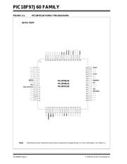
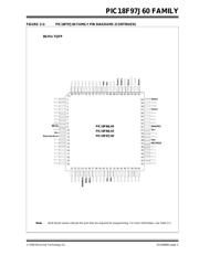
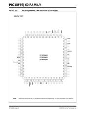
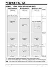
2.1 Pin Diagrams
The pin diagrams for the PIC18F97J60 family are
shown in Figure 2-1 through Figure 2-3. The pins that
are required for programming are listed in Table 2-1
and shown in darker lettering in the figures.
TABLE 2-1: PIN DESCRIPTIONS (DURING PROGRAMMING): PIC18F97J60 FAMILY
• PIC18F66J60 • PIC18F66J65 • PIC18F67J60
• PIC18F86J60 • PIC18F86J65 • PIC18F87J60
• PIC18F96J60 • PIC18F96J65 • PIC18F97J60
Pin Name
During Programming
Pin Name Pin Type Pin Description
MCLR MCLR P Programming Enable
VDD and AVDD
(1)
VDD P Power Supply
VSS and AVSS
(1)
VSS PGround
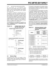
ENVREG ENVREG P Internal Voltage Regulator Enable
V
DDCORE/VCAP VDDCORE P Regulated Power Supply for Microcontroller Core
VCAP I Filter Capacitor for On-Chip Voltage Regulator
RB6 PGC I Serial Clock
RB7 PGD I/O Serial Data
Legend: I = Input, O = Output, P = Power
Note 1: All power supply and ground pins must be connected, including analog and Ethernet supplies (AV
DD,
V
DDPLL, VDDRX, VDDTX) and grounds (AVSS, VSSPLL, VSSRX, VSSTX).
Flash Microcontroller Programming Specification