下载
© 2009 Microchip Technology Inc. Advance Information DS41297F-page 1
PIC18F2XK20/4XK20
1.0 DEVICE OVERVIEW
This document includes the programming
specifications for the following devices:
• PIC18F23K20
• PIC18F24K20
• PIC18F25K20
• PIC18F26K20
• PIC18F43K20
• PIC18F44K20
• PIC18F45K20
• PIC18F46K20
2.0 PROGRAMMING OVERVIEW
The PIC18F2XK20/4XK20 devices can be pro-
grammed using either the high-voltage In-Circuit Serial
Programming™ (ICSP™) method or the low-voltage
ICSP method. Both methods can be done with the
device in the users’ system. The low-voltage ICSP
method is slightly different than the high-voltage
method and these differences are noted where applica-
ble. This programming specification applies to the
PIC18F2XK20/4XK20 devices in all package types.
2.1 Hardware Requirements
In High-Voltage ICSP mode, the PIC18F2XK20/4XK20
devices require two programmable power supplies:
one for V
DD and one for MCLR/VPP/RE3. Both supplies
should have a minimum resolution of 0.25V. Refer to
Section 6.0 “AC/DC Characteristics Timing
Requirements for Program/Verify Test Mode” for
additional hardware parameters.
2.1.1 LOW-VOLTAGE ICSP
PROGRAMMING
In Low-Voltage ICSP mode, the PIC18F2XK20/4XK20
devices can be programmed using a single V
DD source
in the operating range. The MCLR
/VPP/RE3 does not
have to be brought to a different voltage, but can
instead be left at the normal operating voltage. Refer to
Section 6.0 “AC/DC Characteristics Timing
Requirements for Program/Verify Test Mode” for
additional hardware parameters.
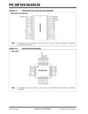
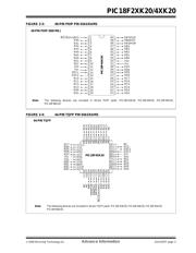
2.2 Pin Diagrams
The pin diagrams for the PIC18F2XK20/4XK20 family
are shown in Figure 2-3 and Figure 2-4.
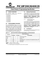
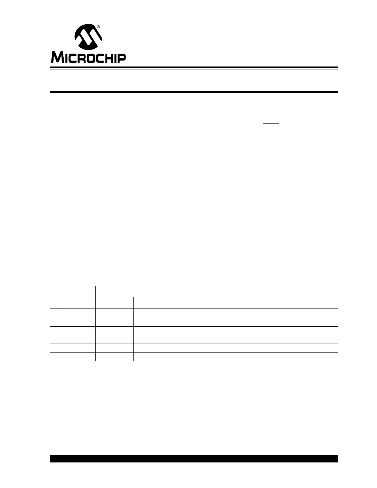
TABLE 2-1: PIN DESCRIPTIONS (DURING PROGRAMMING): PIC18F2XK20/4XK20
Pin Name
During Programming
Pin Name Pin Type Pin Description
MCLR/VPP/RE3 VPP P Programming Enable
V
DD
(2)
VDD P Power Supply
VSS
(2)
VSS PGround
RB5 PGM I Low-Voltage ICSP™ input when LVP
Configuration bit equals ‘1’
(1)
RB6 PGC I Serial Clock
RB7 PGD I/O Serial Data
Legend: I = Input, O = Output, P = Power
Note 1: See Figure 5-1 for more information.
2: All power supply (VDD) and ground (VSS) pins must be connected.
Flash Memory Programming Specification


