下载
2010 Microchip Technology Inc. Advance Information DS41342E-page 1
PIC18F1XK50/PIC18LF1XK50
1.0 DEVICE OVERVIEW
This document includes the programming
specifications for the following devices:
2.0 PROGRAMMING OVERVIEW
The PIC18F1XK50/PIC18LF1XK50 devices can be
programmed using either the high-voltage In-Circuit
Serial Programming™ (ICSP™) method or the low-
voltage ICSP method. Both methods can be done with
the device in the user’s system. The low-voltage ICSP
method is slightly different than the high-voltage
method and these differences are noted where
applicable. The PIC18F1XK50 devices operate from
1.8 to 5.5 volts, and the PIC18LF1XK50 devices
operate from 1.8 to 3.6 volts. All other aspects of the
PIC18F1XK50 with regards to the PIC18LF1XK50
devices are identical.
2.1 Hardware Requirements
In High-Voltage ICSP mode, the PIC18F1XK50/
PIC18LF1XK50 devices require two programmable
power supplies: one for V
DD and one for MCLR/VPP/
RA3. Both supplies should have a minimum resolution
of 0.25V. Refer to Section 8.1 “AC/DC Characteris-
tics Timing Requirements for Program/Verify Test
Mode” for additional hardware parameters.
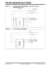
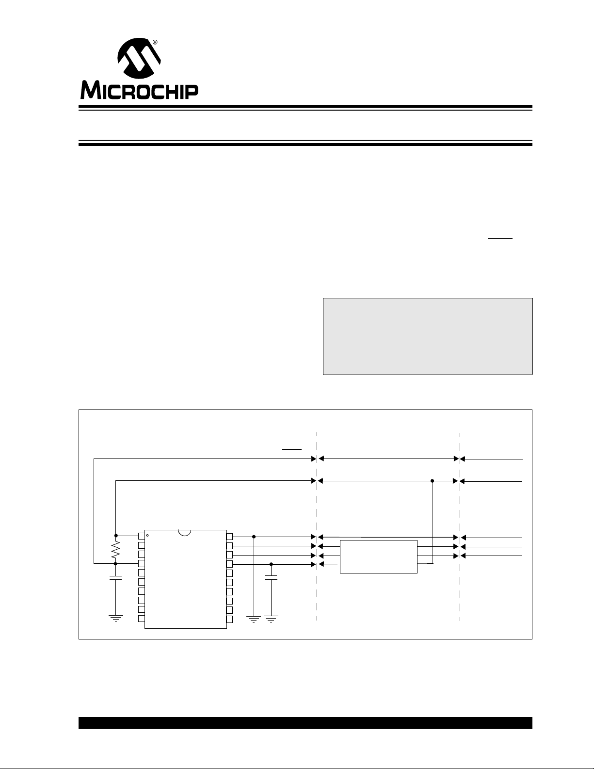
FIGURE 2-1: IN-CIRCUIT SERIAL PROGRAMMING™ (ICSP™) PIC18F1XK50 RECOMMENDED
CIRCUIT
• PIC18F13K50 • PIC18LF13K50
• PIC18F14K50 • PIC18LF14K50
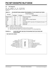
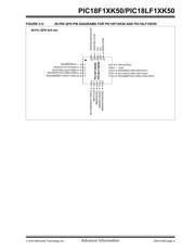
Note: The VIH voltage levels on port pins RA0/
D+/PGD and RA1/D-/PGC must be limited
to 3.3V maximum, due to USB circuitry.
The device must not be attached to a USB
host and the USB module must be
disabled. Refer to Figure 2-1, Figure 2-2
and Figure 2-3.
A
1
A
2
V
2
Bidirectional
Level Translator
Y
1
Y
2
V
1
10
2
3
4
5
6
1
8
7
9
11
12
13
14
15
16
19
20
18
17
VSS
PGD
PGC
VUSB
VSS
ICSPDAT
ICSPCLK
V
PP
+5V
MCLR
VDD
10K
0.1 F
330 nF
Application
Translator
Programmer
PIC18F1XK50
Flash Memory Programming Specification

