下载

© 2005 Microchip Technology Inc. DS41191D-page 1
PIC12F629/675/PIC16F630/676
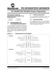
This document includes the
programming specifications for the
following devices:
1.0 PROGRAMMING THE
PIC12F629/675/PIC16F630/676
The PIC12F629/675/PIC16F630/676 is programmed
using a serial method. The Serial mode will allow the
PIC12F629/675/PIC16F630/676 to be programmed
while in the user’s system. This allows for increased
design flexibility. This programming specification
applies to PIC12F629/675/PIC16F630/676 devices in
all packages.
1.1 Hardware Requirements
The PIC12F629/675/PIC16F630/676 requires one
power supply for V
DD (5.0V) and one for VPP (12V).
1.2 Programming Mode
The Programming mode for the PIC12F629/675/
PIC16F630/676 allows programming of user program
memory, data memory, special locations used for ID
and the Configuration Word register.
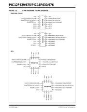
FIGURE 1-1: 8-PIN DIAGRAMS FOR PIC12F629/675
•PIC12F629 •PIC16F630
•PIC12F675 •PIC16F676
PDIP, SOIC
VSSVDD
GP5/T1CKI/OSC1/CLKIN
GP4/AN3/T1G
/OSC2/CLKOUT
GP3/MCLR
/VPP
GP0/AN0/CIN+/ICSPDAT
GP1/AN1/CIN-/V
REF/ICSPCLK
GP2/AN2/T0CKI/INT/COUT
1
2
3
45
6
7
8
PIC12F675
VSS
VDD
GP5/T1CKI/OSC1/CLKIN
GP4/T1G
/OSC2/CLKOUT
GP3/MCLR
/VPP
GP0/CIN+/ICSPDAT
GP1/CIN-/ICSPCLK
GP2/T0CKI/INT/COUT
1
2
3
45
6
7
8
PIC12F629
1
2
3
4
5
6
7
8
PIC12F629
V
SS
GP0/CIN+/ICSPDAT
GP1/CIN-/ICSPCLK
GP2/T0CKI/INT/COUT
VDD
GP5/TICKI/OSC1/CLKIN
GP4/TIG
/OSC2/CLKOUT
GP3/MCLR
/VDD
1
2
3
4
5
6
7
8
PIC12F675
V
SS
GP0/AN0/CIN+/ICSPDAT
GP1/AN1/CIN-/ICSPCLK
GP2/AN2/T0CKI/INT/COUT
VDD
GP5/TICKI/OSC1/CLKIN
GP4/AN4/TIG
/OSC2/CLKOUT
GP3/MCLR
/VDD
DFN, DFN-S
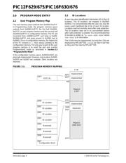
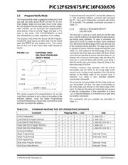
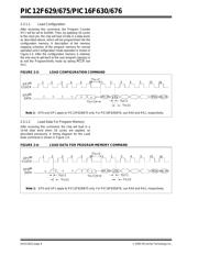
PIC12F629/675/PIC16F630/676 Memory Programming

