

下载
2011-2012 Microchip Technology Inc. Advance Information DS41561C-page 1
PIC12F752/HV752
1.0 DEVICE OVERVIEW
This document includes the programming
specifications for the following devices:
2.0 PROGRAMMING THE
PIC12F752/HV752 DEVICES
The PIC12F752/HV752 devices are programmed using a
serial method. The Serial mode will allow these devices to
be programmed while in the user’s system. These
programming specifications apply to all of the above
devices in all packages.
2.1 Hardware Requirements
These devices require one power supply for VDD, see
Table 7-1 V
DD, and one for VPP, see Tabl e 7- 1 VIHH.
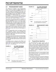
2.2 Program/Verify Mode
The Program/Verify mode for these devices allows
programming of user program memory, user ID
locations, Calibration Word and the Configuration
Word.
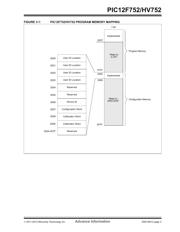
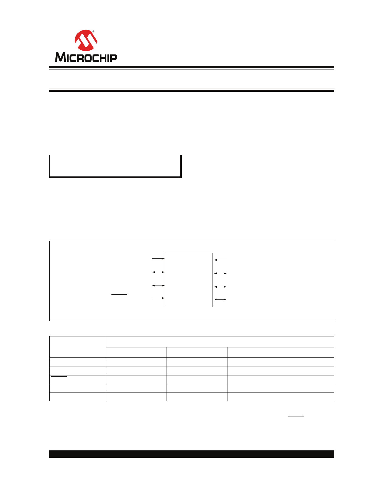
FIGURE 2-1: 8-PIN PROGRAMMING PIN DIAGRAM FOR PIC12F752/HV752
TABLE 2-1: PIN DESCRIPTIONS IN PROGRAM/VERIFY MODE: PIC12F752/HV752
•PIC12F752 •PIC12HV752
Note 1: All references to the PIC12F752 parts
refer to the PIC12HV752 parts as well
(unless otherwise specified).
Pin Name
During Programming
Function Pin Type Pin Description
RA1 ICSPCLK I Clock input – Schmitt Trigger input
RA0 ICSPDAT I/O Data input/output – Schmitt Trigger input
MCLR
Program/Verify mode P
(1)
Program Mode Select
VDD VDD P Power Supply
V
SS VSS PGround
Legend: I = Input, O = Output, P = Power
Note 1: In the PIC12F752/HV752, the programming high voltage is internally generated. To activate the Program/
Verify mode, voltage of V
IHH and a current of IIHH (see Table 7-1) need to be applied to MCLR input.
1
2
3
4
5
6
7
8
PIC12F752/HV752
VSS
RA0/ICSPDAT
RA1/ICSPCLK
RA2
MCLR/VPP/RA3
VDD
RA5
RA4
Flash Memory Programming Specification