


下载
10kW
ADC
G=1
R
F
R
I
Output
Stage
SPI
Interface
SCLK
DIO
CS
7
V
OUT
5
DV
DD
10
AV
DD
1
GND
6
V
REF
4
3
8
9
MSP430
Microcontroller
+3V
+5V
V
REF
PGA112
PGA113
V /CH0
CAL
2
CH1
CAL3
CAL4
CAL1
CAL2
0.1V
CAL
0.9V
CAL
10kW
80kW
MUX
CAL2/3
C
0.1 F
BYPASS
m
C
0.1 F
BYPASS
m
C
0.1 F
BYPASS
m
Product
Folder
Sample &
Buy
Technical
Documents
Tools &
Software
Support &
Community
Reference
Design
PGA112
,
PGA113
,
PGA116
,
PGA117
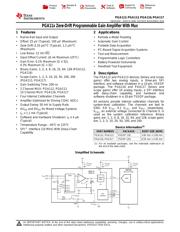
SBOS424C –MARCH 2008–REVISED NOVEMBER 2015
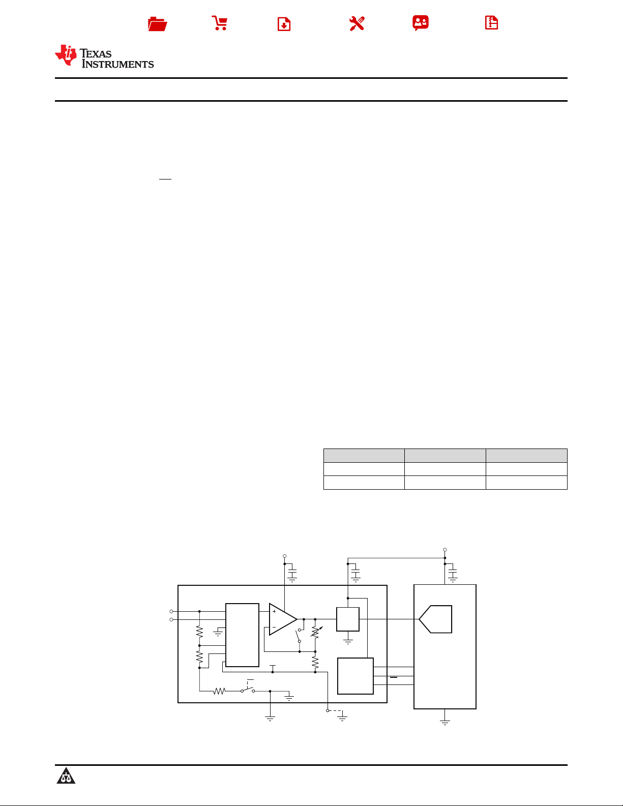
PGA11x Zerø-Drift Programmable Gain Amplifier With Mux
1 Features 2 Applications
1
• Rail-to-Rail Input and Output
• Remote e-Meter Reading
• Offset: 25 μV (Typical), 100 μV (Maximum) • Automatic Gain Control
• Zerø Drift: 0.35 μV/°C (Typical), 1.2 μV/°C • Portable Data Acquisition
(Maximum)
• PC-Based Signal Acquisition Systems
• Low Noise: 12 nV/√Hz
• Test and Measurement
• Input Offset Current: ±5 nA Maximum (25°C)
• Programmable Logic Controllers
• Gain Error: 0.1% Maximum (G ≤ 32),
• Battery-Powered Instruments
0.3% Maximum (G > 32)
• Handheld Test Equipment
• Binary Gains: 1, 2, 4, 8, 16, 32, 64, 128 (PGA112,
PGA116)
3 Description
• Scope Gains: 1, 2, 5, 10, 20, 50, 100, 200
The PGA112 and PGA113 devices (binary and scope
(PGA113, PGA117)
gains) offer two analog inputs, a three-pin SPI
interface, and software shutdown in a 10-pin, VSSOP
• Gain Switching Time: 200 ns
package. The PGA116 and PGA117 (binary and
• 2 Channel MUX: PGA112, PGA113
scope gains) offer 10 analog inputs, a SPI interface
10 Channel MUX: PGA116, PGA117
with daisy-chain capability, and hardware and
• Four Internal Calibration Channels
software shutdown in a 20-pin TSSOP package.
• Amplifier Optimized for Driving CDAC ADCs
All versions provide internal calibration channels for
• Output Swing: 50 mV to Supply Rails system-level calibration. The channels are tied to
GND, 0.9 V
CAL
, 0.1 V
CAL
, and V
REF
, respectively.
• AV
DD
and DV
DD
for Mixed Voltage Systems
V
CAL
, an external voltage connected to Channel 0, is
• I
Q
= 1.1 mA (Typical)
used as the system calibration reference. Binary
• Software and Hardware Shutdown: I
Q
≤ 4 μA
gains are: 1, 2, 4, 8, 16, 32, 64, and 128; scope gains
(Typical)
are: 1, 2, 5, 10, 20, 50, 100, and 200.
• Temperature Range: –40°C to 125°C
Device Information
(1)
• SPI™ Interface (10 MHz) With Daisy-Chain
PART NUMBER PACKAGE BODY SIZE (NOM)
Capability
PGA112, PGA113 VSSOP (10) 3.00 mm × 3.00 mm
PGA116, PGA117 TSSOP (20) 6.50 mm × 4.40 mm
(1) For all available packages, see the orderable addendum at
the end of the data sheet.
Simplified Schematic
1
An IMPORTANT NOTICE at the end of this data sheet addresses availability, warranty, changes, use in safety-critical applications,
intellectual property matters and other important disclaimers. PRODUCTION DATA.
页面指南