
下载

Maxim > Design Support > Technical Documents > Tutorials > A/D and D/A Conversion/Sampling Circuits > APP 3189
Keywords: Handbook, programming,
MAX5592,MAX5293,MAX5581,MAX5291,MAX5294,MAX5583,MAX5585,MAX5591,MAX5593,MAX5595,MAX5590-
95,MAX5295,MAX5580-85,MAX5292,MAX5290,MAX5580,MAX5582,MAX5584,MAX5590,MAX5594
TUTORIAL 3189
Programmers Handbook for the MAX5290-MAX5295,
MAX5580-MAX5585, MAX5590-MAX5595 User-
Programmable DACs
Jun 27, 2004
Abstract: The Programmers Handbook provides detailed timing patterns and advanced programming features for
the MAX5290-MAX5295, MAX5580-MAX5585, MAX5590-MAX5595 user-programmable D/A converters (DACs).
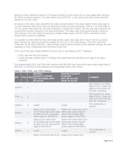
This handbook provides detailed timing patterns and advanced programming features for the MAX5290-
MAX5295, MAX5580-MAX5585, and MAX5590-MAX5595 user-programmable D/A converters (DACs). Each
device in this family shares a common, highly flexible, 3-, 4-, or 5- wire serial interface. The inputs and outputs
which make up the interface are:
SCLK - serial clock input. Data may be clocked into, and out of, the serial interface on either rising or falling
clock edges, depending on configuration.
DIN - serial data input.
CS - active-low chip select. For all modes except the DSP Frame Sync mode, the falling edge of CS
corresponds to the start of the serial interface command, and the rising edge of CS corresponds to the end
of the command.
DSP - DSP is sampled at the end of the power-on reset sequence, and its state determines the active edge
of the SCLK signal for clocking in data at DIN. Connect DSP to DV
DD
to clock in data on the rising edge of
SCLK, or connect to DGND to clock in data on the falling edge of SCLK. DSP may also be actively driven, in
which case the first rising edge of DSP after the power-on reset will enable the DSP Frame Sync mode.
UPIO1/UPIO2 - Each device in the family has two user-programmable I/O ports (UPIO1 and UPIO2) which
can be configured in a variety of modes including serial output data ports, either for read-back (DOUTRB) or
daisy-chaining (DOUTDC0 or DOUTDC1).
Please refer to the MAX5290-MAX5295, MAX5580-MAX5585, or MAX5590-MAX5595 datasheets for details on
timing specifications and device configurations.
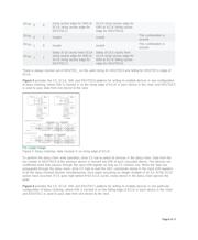
Any device within the family is capable of supporting a wide range of configurations, including (but not limited to)
the following:
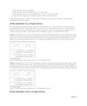
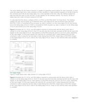
Write operation to a single device
Page 1 of 11