
下载

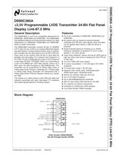
DS90C385A
+3.3V Programmable LVDS Transmitter 24-Bit Flat Panel
Display Link-87.5 MHz
General Description
The DS90C385A is a pin to pin compatible replacement for
DS90C383, DS90C383A and DS90C385. The DS90C385A
has additional features and improvements making it an ideal
replacement for DS90C383, DS90C383A and DS90C385.
family of LVDS Transmitters.
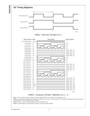
The DS90C385A transmitter converts 28 bits of LVCMOS/
LVTTL data into four LVDS (Low Voltage Differential Signal-
ing) data streams. A phase-locked transmit clock is transmit-
ted in parallel with the data streams over the fifth LVDS link.
Every cycle of the transmit clock 28 bits of input data are
sampled and transmitted. At a transmit clock frequency of
87.5 MHz, 24 bits of RGB data and 3 bits of LCD timing and
control data (FPLINE, FPFRAME, DRDY) are transmitted at
a rate of 612.5Mbps per LVDS data channel. Using a 87.5
MHz clock, the data throughput is 306.25Mbytes/sec. This
transmitter can be programmed for Rising edge strobe or
Falling edge strobe through a dedicated pin. A Rising edge
or Falling edge strobe transmitter will interoperate with a
Falling edge strobe FPDLink Receiver without any transla-
tion logic.
This chipset is an ideal means to solve EMI and cable size
problems associated with wide, high-speed TTL interfaces
with added Spread Spectrum Clocking support.
Features
n Pin-to-pin compatible to DS90C383, DS90C383A and
DS90C385 .
n No special start-up sequence required between
clock/data and /PD pins. Input signals (clock and data)
can be applied either before or after the device is
powered.
n Support Spread Spectrum Clocking up to 100kHz
frequency modulation & deviations of
±
2.5% center
spread or -5% down spread.
n “Input Clock Detection” feature will pull all LVDS pairs to
logic low when input clock is missing and when /PD pin
is logic high.
n 18 to 87.5 MHz shift clock support
n Tx power consumption
<
147 mW (typ)
@
87.5 MHz
Grayscale
n Tx Power-down mode
<
60 µW (typ)
n Supports VGA, SVGA, XGA, SXGA(dual pixel),
SXGA+(dual pixel), UXGA(dual pixel).
n Narrow bus reduces cable size and cost
n Up to 2.45 Gbps throughput
n Up to 306.25Megabytes/sec bandwidth
n 345 mV (typ) swing LVDS devices for low EMI
n PLL requires no external components
n Compliant to TIA/EIA-644 LVDS standard
n Low profile 56-lead TSSOP package
Block Diagram
DS90C385A
20070201
Order Number DS90C385AMT
See NS Package Number MTD56
April 2006
DS90C385A +3.3V Programmable LVDS Transmitter 24-bit Flat Panel Display (FPD) Link-87.5 MHz
© 2006 National Semiconductor Corporation DS200702 www.national.com
页面指南