


下载
CY8C21345
CY8C22345
CY8C22545
PSoC
®
Programmable System-on-Chip
Cypress Semiconductor Corporation • 198 Champion Court • San Jose, CA 95134-1709 • 408-943-2600
Document Number: 001-43084 Rev. *V Revised December 17, 2014
Features
■ Powerful Harvard-architecture processor:
❐ M8C processor speeds up to 24 MHz
❐ 8 × 8 multiply, 32-bit accumulate
❐ Low power at high speed
❐ 3.0 V to 5.25 V operating voltage
❐ Industrial temperature range: –40 °C to +85 °C
■ Advanced peripherals (PSoC
®
Blocks)
❐ Six analog type “E” PSoC blocks provide:
• Single or dual 8-Bit ADC
• Comparators (up to four)
❐ Up to eight digital PSoC blocks provide:
• 8- to 32-bit timers and counters, 8- and 16-bit pulse-width
modulators (PWMs)
• One shot, multi-shot mode support in timers and PWMs
• PWM with deadband support in one digital block
• Shift register, CRC, and PRS modules
• Full duplex UART
• Multiple SPI masters or slaves, variable data length
Support: 8- to 16-Bit
• Can be connected to all GPIO pins
❐ Complex peripherals by combining blocks
❐ Shift function support for FSK detection
❐ Powerful synchronize feature support. Analog module
operations can be synchronized by digital blocks or external
signals.
■ High speed 10-bit SAR ADC with sample and hold optimized for
embedded control
■ Precision, programmable clocking:
❐ Internal ± 5%
[1]
24/48 MHz oscillator across the industrial
temperature range
❐ High accuracy 24 MHz with optional 32 kHz crystal and PLL
❐ Optional external oscillator, up to 24 MHz
❐ Internal/external oscillator for watchdog and sleep
■ Flexible on-chip memory:
❐ Up to 16 KB flash program storage 50,000 erase/write cycles
❐ Up to 1-KB SRAM data storage
❐ In-system serial programming (ISSP)
❐ Partial flash updates
❐ Flexible protection modes
❐ EEPROM emulation in flash
■ Optimized CapSense
®
resource:
❐ Two IDAC support up to 640 µA source current to replace
external resistor
❐ Two dedicated clock resources for CapSense:
• CSD_CLK: 1/2/4/8/16/32/128/256 derive from SYSCLK
• CNT_CLK: 1/2/4/8 Derive from CSD_CLK
❐ Dedicated 16-bit timers/counters for CapSense scanning
❐ Support dual CSD channels simultaneous scanning
■ Programmable pin configurations:
❐ 25 mA sink, 10 mA source on all GPIOs
❐ Pull-up, pull-down, high Z, Strong, or open-drain drive modes
on all GPIOs
❐ Up to 38 analog inputs on GPIOs
❐ Configurable interrupt on all GPIOs
■ Additional system resources:
❐ I
2
C slave, master, and multimaster to 400 kHz
❐ Supports hardware addressing feature
❐ Watchdog and sleep timers
❐ User configurable low voltage detection
❐ Integrated supervisory circuit
❐ On-Chip precision voltage reference
❐ Supports RTC block into digital peripheral logic
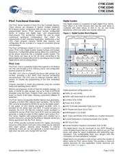
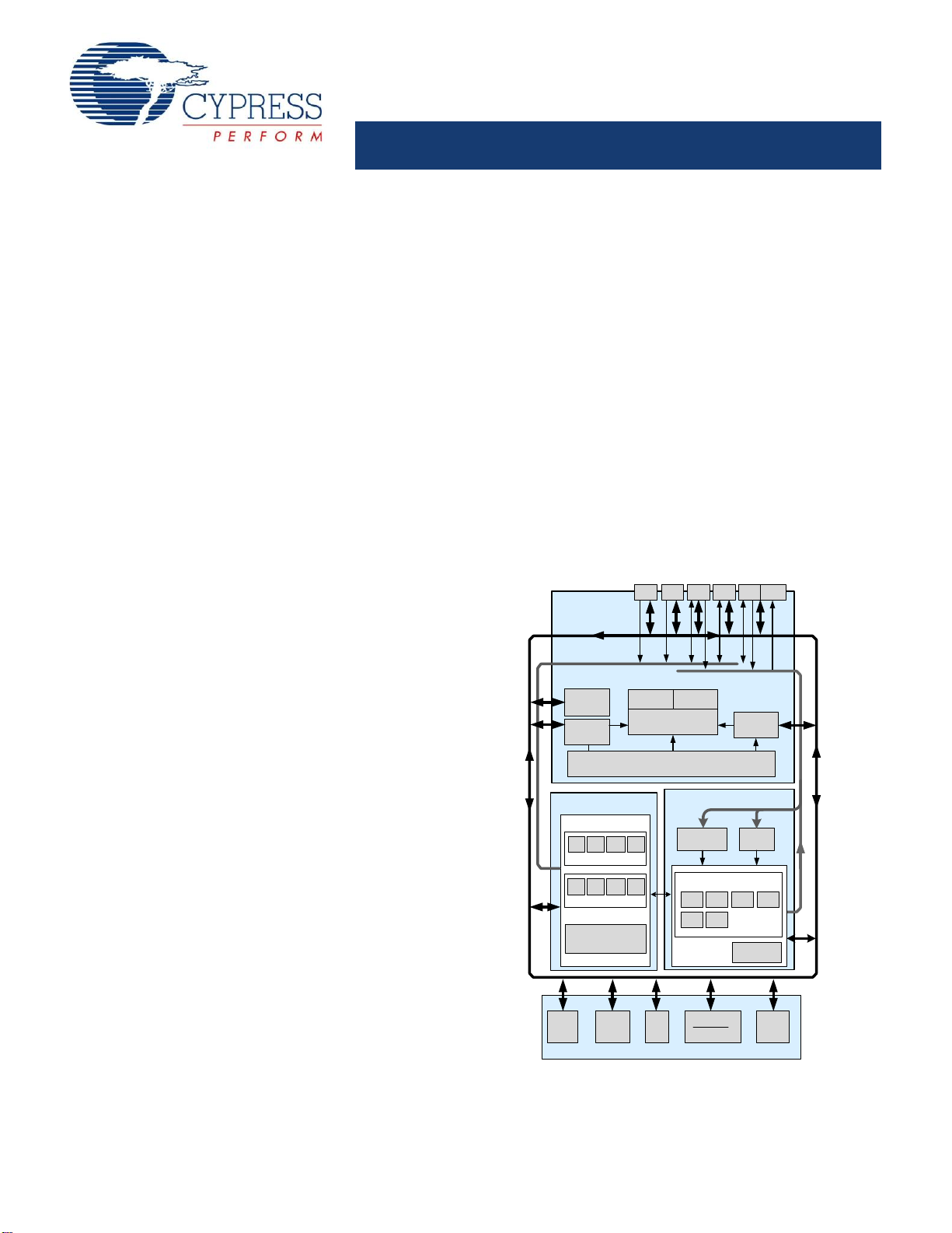
Top Level Block Diagram
DIGITAL SYSTEM
Digital Block Array
DBC DBC
DCC DCC
ROW 1
DBC DBC DCC DCC
ROW 2
SRAM
1K
Interrupt
Controller
Sleep and
Watchdog
Multiple Clock Sources
(Includes IMO, ILO, PLL, and ECO)
Global Digital Interconnect
Global Analog Interconnect
CPU Core (M8C)
SROM Flash 16K
MACs
Internal
Voltage
Ref.
Digital
Clocks
POR and LVD
System Resets
SYSTEM RESOURCES
ANALOG SYSTEM
Analog
Ref
Analog Input
Muxing(L,R)
=
Port 2 Port 1 Port 0
Analog
Drivers
10-bit SAR
ADC
Port 3
Port 4
PSoC Core
I
2
C
System Bus
CTE CTE
Analog Block Array
CTE CTE
SCE SCE
CapSense
Digital Resource
Errata: For information on silicon errata, see “Errata” on page 35. Details include trigger conditions, devices affected, and proposed workaround.
Note
1. Errata: When the device is operated within 0 °C to 70 °C, the frequency tolerance is reduced to ±2.5%, but if operated at extreme temperature (below 0 °C or above
70 °C), frequency tolerance deviates from ±2.5% to ±5%. For more information, see “Errata” on page 35.
页面指南