
下载
CY8C21123/CY8C21223/CY8C21323
PSoC
®
Programmable System-on-Chip™
Cypress Semiconductor Corporation • 198 Champion Court • San Jose, CA 95134-1709 • 408-943-2600
Document Number: 38-12022 Rev. AA Revised January 18, 2016
Features
■ Powerful Harvard-architecture processor:
❐ M8C processor speeds up to 24 MHz
❐ Low power at high speed
❐ Operating voltage: 2.4 V to 5.25 V
❐ Operating voltages down to 1.0 V using on-chip switch mode
pump (SMP)
❐ Industrial temperature range: –40 °C to +85 °C
■ Advanced peripherals (PSoC
®
blocks):
❐ Four analog type “E” PSoC blocks provide:
• Two comparators with digital to analog converter (DAC)
references
• Single or dual 10-Bit 8-to-1 analog to digital converter
(ADC)
❐ Four digital PSoC blocks provide:
• 8- to 32-bit timers and counters, 8- and 16-bit pulse-width
modulators (PWMs)
• CRC and PRS modules
❐ Full duplex UART, SPI master or slave: Connectable to all
general-purpose I/O (GPIO) pins
❐ Complex peripherals by combining blocks
■ Flexible on-chip memory:
❐ 4 KB flash program storage 50,000 erase/write cycles
❐ 256 bytes SRAM data storage
❐ In-system serial programming (ISSP)
❐ Partial flash updates
❐ Flexible protection modes
❐ EEPROM emulation in flash
■ Complete development tools:
❐ Free development software (PSoC Designer™)
❐ Full-featured, in-circuit emulator (ICE) and programmer
❐ Full-speed emulation
❐ Complex breakpoint structure
❐ 128-KB trace memory
■ Precision, programmable clocking:
❐ Internal ±5% 24- / 48-MHz main oscillator
❐ Internal low-speed, low-power oscillator for watchdog and
sleep functionality
■ Programmable pin configurations:
❐ 25-mA sink, 10-mA source on all GPIOs
❐ Pull-up, pull-down, high Z, strong, or open-drain drive modes
on all GPIOs
❐ Up to eight analog inputs on all GPIOs
❐ Configurable interrupt on all GPIOs
■
■
Additional system resources:
❐ I
2
C master, slave and multi-master to 400 kHz
❐ Watchdog and sleep timers
❐ User-configurable low-voltage detection (LVD)
❐ Integrated supervisory circuit
❐ On-chip precision voltage reference
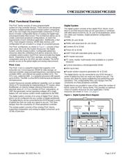
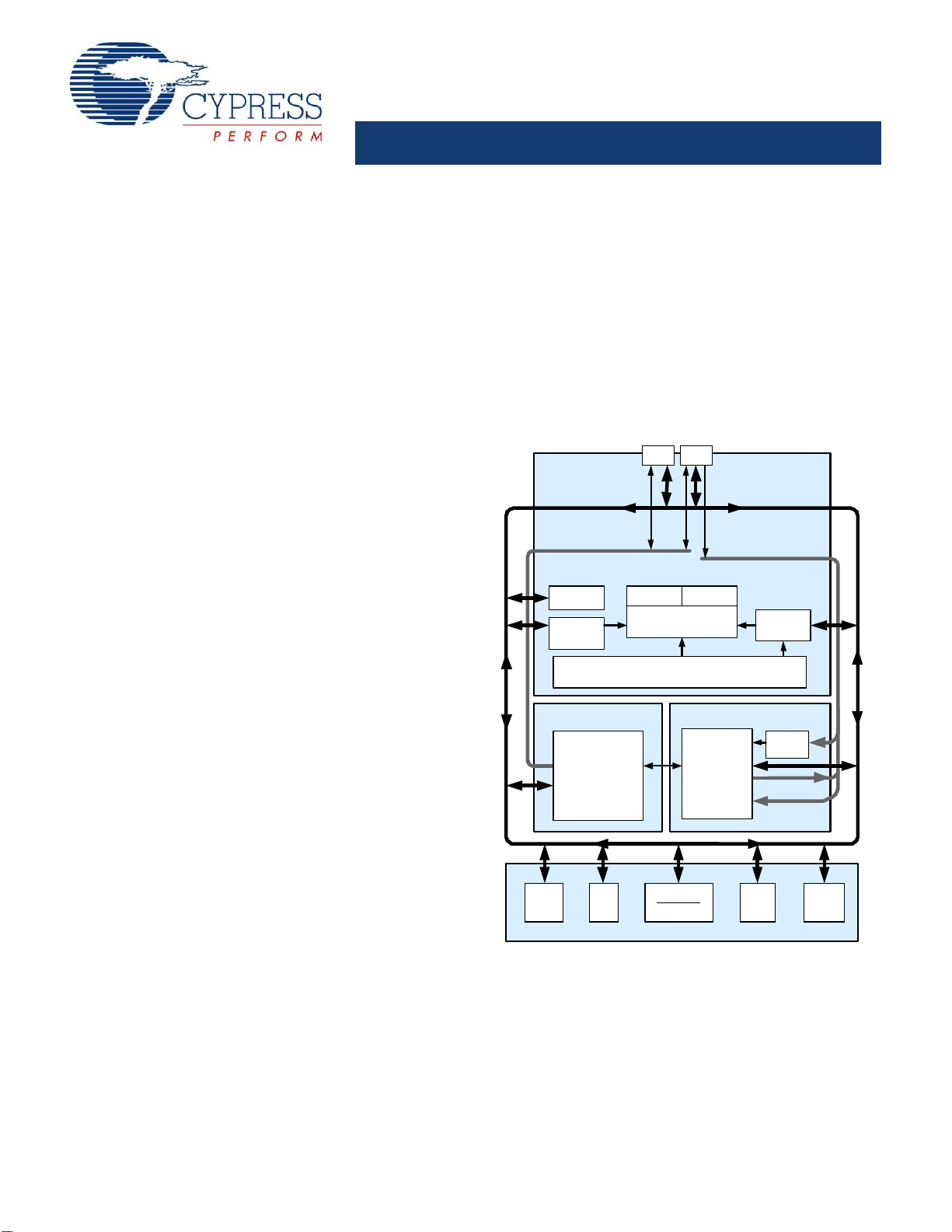
Logic Block Diagram
DIGITAL SYSTEM
SRAM
System Bus
Interrupt
Controller
Sleep and
Watchdog
Clock Source s
(Includes IMO and ILO)
Global Digital Interconnect
Global Analog Interconnect
PSoC
CORE
CPU Core
(M8C)
SROM Flash
I2C
Internal
Voltage
Ref .
Digital
Cloc ks
POR and LVD
System Resets
SYSTEM RESOURCES
ANALOG SYSTEM
Analog
Ref .
Port 1 Port 0
Digital
PSoC Block
Array
Analog
PSoC Block
Array
Sw itch
Mode
Pump
Errata: When the device is operated within 0 °C to 70 °C, the frequency tolerance is reduced to ±2.5%, but if operated at extreme temperature (below 0 °C or above 70 °C),
frequency tolerance deviates from ±2.5% to ±5%. For information on silicon errata, see “Errata” on page 43.
页面指南