


CY25200
Programmable Spread Spectrum
Clock Generator for EMI Reduction
Cypress Semiconductor Corporation • 198 Champion Court • San Jose, CA 95134-1709 • 408-943-2600
Document Number: 38-07633 Rev. *L Revised November 24, 2016
Programmable Spread Spectrum Clock Generator for EMI Reduction
Features
■ Wide Operating Output (SSCLK) Frequency Range
❐ 3 to 200 MHz
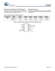
■ Programmable Spread Spectrum with Nominal 31.5 kHz
modulation Frequency
■ Center Spread: ±0.25% to ±2.5%
■ Down Spread: –0.5% to –5.0%
■ Input Frequency Range
❐ External crystal: 8 to 30 MHz fundamental crystals
❐ External reference: 8 to 166 MHz clock
■ Integrated Phase-Locked Loop (PLL)
■ Programmable Crystal Load Capacitor Tuning Array
■ Low Cycle-to-Cycle Jitter
■ 3.3 V Operation with 2.5 V Output Clock Drive Option
■ Spread Spectrum On and Off Function
■ Power Down or Output Enable Function
■ Output Frequency Select Option
■ Field-Programmable
■ Package: 16-pin TSSOP
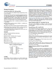
Functional Description
The CY25200 is a programmable clock generator with spread
spectrum capability. Spread spectrum modulates the output
clock frequency over a small range, spreading the energy and
reducing the energy peak. This is a powerful technique to reduce
EMI in a variety of applications.
It uses either an external reference clock or a crystal for an input.
It also uses a PLL to generate a spread spectrum output clock
that can be a different frequency than the input. Up to six output
clocks are available and up to two of them can be REFCLKs
(copies of the input clock, without spread).
The CY25200 is highly configurable. Programmable variables
include the input and output frequencies, spread percentage,
center spread or down spread, and control pin functions. The
oscillator pin capacitance can also be programmed to match the
load capacitance requirement (C
L
) of the crystal, eliminating the
need for external capacitors.
Available features include Output Enable, Power Down, Spread
On/Off, Frequency Select, and the option to power some output
clocks at 2.5 V.
Programmability enables fast prototyping, which is particularly
useful when doing EMC testing and determining the optimal
spread settings.
For a complete list of related documentation, click here.
Divider
PLL
SSCLK3
Q
P
VCO
SSCLK2
SSCLK4
SSCLK5/REFOUT/CP2
SSCLK6/REFOUT/CP3
Bank 1
Divider
Bank 2
Output
Select
SSCLK1
Matrix
VDDL
AVSS
AVDD
VSS
VSSLVDD
CP0
CP1
2
35
13
11
6
410
7
8
9
12
14
15
XIN/CLKIN
OSC.
XOUT
C
XIN
1
C
XOUT
16
Logic Block Diagram
页面指南