


下载
CY22392
Three-PLL General Purpose
Flash Programmable Clock Generator
Cypress Semiconductor Corporation • 198 Champion Court • San Jose, CA 95134-1709 • 408-943-2600
Document Number: 38-07013 Rev. *K Revised December 18, 2014
Three-PLL Ge neral Purpose FL ASH Programm able Clock Gen erator
Features
■ Three Integrated Phase-locked Loops
■ Ultra Wide Divide Counters (8-bit Q, 11-bit P, and 7-bit Post
Divide)
■ Improved Linear Crystal Load Capacitors
■ Flash Programmability
■ Field Programmable
■ Low-jitter, High-accuracy Outputs
■ Power Management Options (Shutdown, OE, Suspend)
■ Configurable Crystal Drive Strength
■ Frequency Select through three External LVTTL Inputs
■ 3.3 V Operation
■ 16-pin TSSOP and SOIC Packages
■ CyClocksRT™ Support
Benefits
■ Generates up to three unique frequencies on six outputs up to
200 MHz from an external source. Functional upgrade for
current CY2292 family.
■ Enables 0 ppm frequency generation and frequency
conversion under the most demanding applications.
■ Improves frequency accuracy over temperature, age, process,
and initial offset.
■ Nonvolatile programming enables easy customization, fast
turnaround, performance tweaking, design timing margin
testing, inventory control, lower part count, and more secure
product supply. In addition, any part in the family can also be
programmed multiple times, which reduces programming
errors and provides an easy upgrade path for existing designs.
■ In-house programming of samples and prototype quantities is
available using the CY3672 development kit. Production
quantities are available through Cypress Semiconductor’s
value added distribution partners or by using third party
programmers from BP Microsystems, HiLo Systems, and
others.
■ Performance suitable for high-end multimedia,
communications, industrial, A/D Converters, and consumer
applications.
■ Supports numerous low power application schemes and
reduces EMI by enabling unused outputs to be turned off.
■ Adjusts crystal drive strength for compatibility with virtually all
crystals.3-bit external frequency select options for PLL1, CLKA,
and CLKB.
■ Industry-standard supply voltage.Industry-standard packaging
saves on board space.Easy to use software support for design
entry.
■ For a complete list of related documentation, click here.
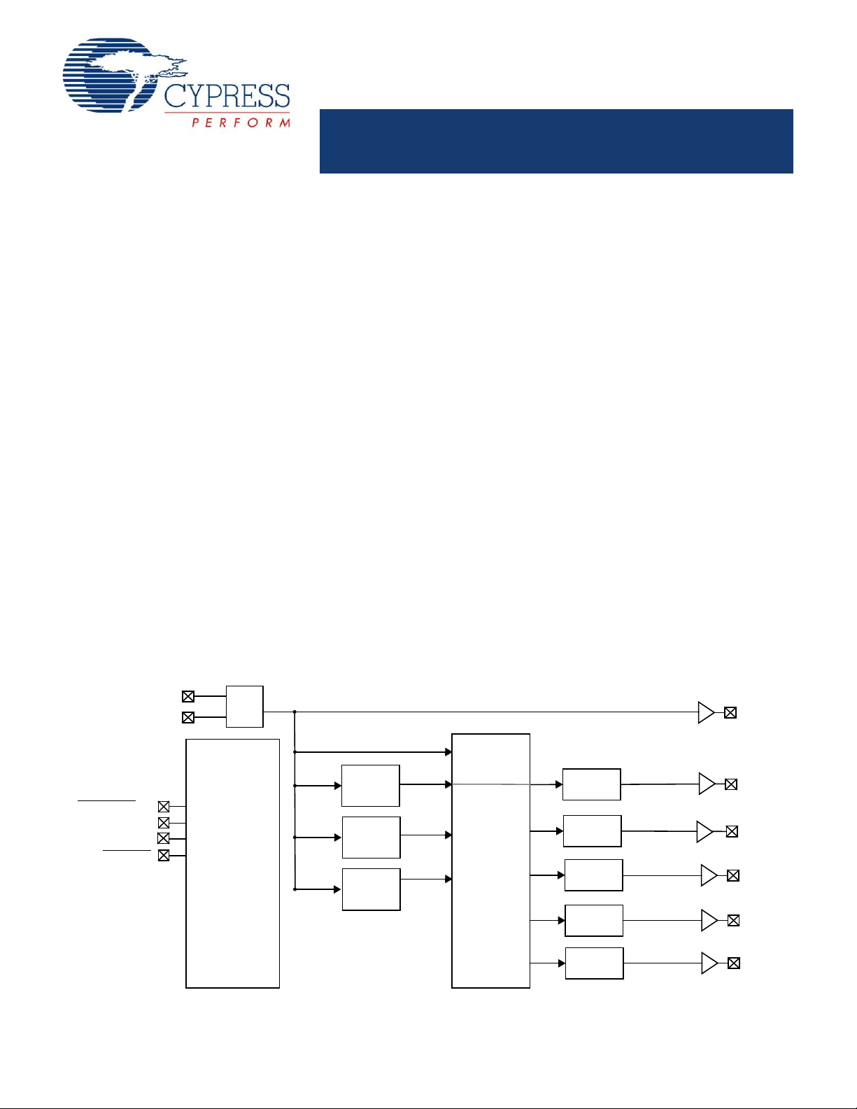
XTALIN
XTALOUT
S2/SUSPEND
S1
S0
SHUTDOWN
/OE
CONFIGURATION
FLASH
OSC.
XBUF
PLL1
CLKE
11 BIT P
8 BIT Q
PLL2
11 BIT P
8 BIT Q
PLL3
11 BIT P
8 BIT Q
4x4
Switch
Crosspoint
Divider
7 BIT
Divider
7 BIT
Divider
7 BIT
Divider
7 BIT
Divider
/2,3, or 4
CLKA
CLKB
CLKC
CLKD
Logic Block Diagram