

下载
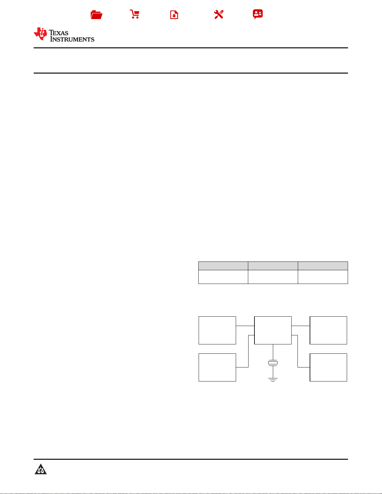
CDCE(L)9xx ClockEthernet PHY
USB Controller
WiFi
FPGA
25 MHz
Copyright © 2016, Texas Instruments Incorporated
Product
Folder
Sample &
Buy
Technical
Documents
Tools &
Software
Support &
Community
An IMPORTANT NOTICE at the end of this data sheet addresses availability, warranty, changes, use in safety-critical applications,
intellectual property matters and other important disclaimers. PRODUCTION DATA.
CDCE937
,
CDCEL937
SLAS564G –AUGUST 2007–REVISED OCTOBER 2016
CDCEx937 Flexible Low Power LVCMOS Clock Generator
With SSC Support For EMI Reduction
1
1 Features
1
• Member of Programmable Clock Generator
Family
– CDCEx913: 1-PLL, 3 Outputs
– CDCEx925: 2-PLL, 5 Outputs
– CDCEx937: 3-PLL, 7 Outputs
– CDCEx949: 4-PLL, 9 Outputs
• In-System Programmability and EEPROM
– Serial Programmable Volatile Register
– Nonvolatile EEPROM to Store Customer
Setting
• Flexible Input Clocking Concept
– External Crystal: 8 MHz to 32 MHz
– On-Chip VCXO: Pull Range ±150 ppm
– Single-Ended LVCMOS up to 160 MHz
• Free Selectable Output Frequency up to 230 MHz
• Low-Noise PLL Core
– PLL Loop Filter Components Integrated
– Low Period Jitter (Typical 60 ps)
• Separate Output Supply Pins
– CDCE937: 3.3 V and 2.5 V
– CDCEL937: 1.8 V
• Flexible Clock Driver
– Three User-Definable Control Inputs
[S0/S1/S2], for Example, SSC Selection,
Frequency Switching, Output Enable or Power
Down
– Generates Highly Accurate Clocks for Video,
Audio, USB, IEEE1394, RFID, Bluetooth™,
WLAN, Ethernet™, and GPS
– Generates Common Clock Frequencies Used
With TI-DaVinci™, OMAP™, DSPs
– Programmable SSC Modulation
– Enables 0-PPM Clock Generation
• 1.8-V Device Power Supply
• Wide Temperature Range –40°C to 85°C
• Packaged in TSSOP
• Development and Programming Kit for Easy PLL
Design and Programming (TI Pro-Clock™)
2 Applications
D-TVs, STBs, IP-STBs, DVD Players, DVD
Recorders, and Printers
3 Description
The CDCE937 and CDCEL937 devices are modular
PLL-based low cost, high-performance,
programmable clock synthesizers, multipliers and
dividers. They generate up to 7 output clocks from a
single input frequency. Each output can be
programmed in-system for any clock frequency up to
230 MHz, using up to three independent configurable
PLLs.
The CDCEx937 has separate output supply pins,
VDDOUT, which is 1.8 V for CDCEL937 and to 2.5 V
to 3.3 V for CDCE937.
The input accepts an external crystal or LVCMOS
clock signal. If an external crystal is used, an on-chip
load capacitor is adequate for most applications. The
value of the load capacitor is programmable from 0 to
20 pF. Additionally, an on-chip VCXO is selectable
which allows synchronization of the output frequency
to an external control signal, that is, PWM signal.
Device Information
(1)
PART NUMBER PACKAGE BODY SIZE (NOM)
CDCE937,
CDCEL937
TSSOP (20) 6.50 mm x 4.40 mm
(1) For all available packages, see the orderable addendum at
the end of the datasheet.
Typical Application Schematic
页面指南