
下载
© Semiconductor Components Industries, LLC, 2015
November, 2015 - Rev. 2
1 Publication Order Number:
AND9331/D
AND9331/D
AX8052 Serial Boot Loader
Introduction
Many products need the ability to update the firmware in
the field. A solution to this requirement is the use of a boot
loader, a small program located in the microcontroller
firmware that communicates with an external entity, such as
a technician’s personal computer. The boot loader, when
activated, receives an updated application firmware and
stores it into the microcontroller flash. On next restart of the
microcontroller, the updated firmware receives control.
This application note describes a simple boot loader that
communicates to the external entity using the serial port
UART0. It is intended as a building block for user’s special
purpose boot loaders.
The boot loader communicates using 38400 Baud, 8 Bits,
1 Stop bit and no parity bits. The transmit signal is output on
PB4, receive signal is expected on PB5. Upon reset, the boot
loader takes control. If Switch 5 is not pressed and an
application firmware has been stored in the flash, it passes
control immediately to the application firmware. If no
application firmware is stored or Switch 5 is pressed, the
boot loader starts and outputs a banner. A simple protocol is
then used to communicate with the boot loader:
Command Description
? Output Banner
K Erase (“Kill”) Application
Z Check whether the Application Area is Erased
(“Zeroed”)
: Start of an Intel Hex file line. The line is parsed
and written into the Application Area. The Applica-
tion Area must have been erased before.
R Run Application
V VDDIO Measurement
A typical Boot Loader Session would therefore look like:
1. “?” − to check communication with the boot loader
2. “K” − to erase the application area
3. Upload the .hex file produced by the (SDCC)
compiler
4. “R” − to run the application
Code Overview
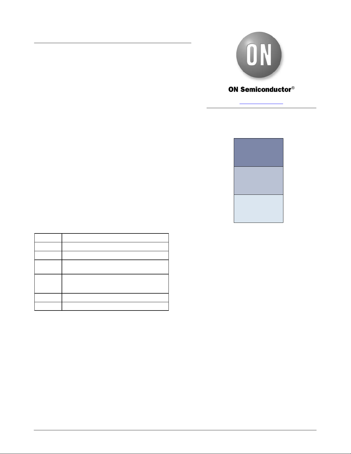
Memory Layout
In order to minimize the constraints on the application, the
boot loader is placed at the end of the memory, just before
the calibration sector. The only constraint on the application
code is that it may not overflow into the boot loader code,
and that it must place a jump instruction at address 0, the
reset vector.
The memory layout looks like this:
Figure 1.
FFFF
FC00
Calibration
Sector
FBFF
E7FE
Boot
Loader
E7FD
0000
Application
Code
Interrupt Vector Table
In order to avoid interrupt overhead for the application,
the boot loader does not use any interrupts. It operates the
UART in a polled fashion.
The boot loader however has to intercept the reset vector.
The boot loader prevents writes to addresses
0x0000–0x0002; instead, it extracts the target address and
writes it to the address 0xE7FE. The boot loader stores its
own reset vector into addresses 0x0000– 0x0002.
After reset, the microcontroller thus jumps into the boot
loader code. The boot loader then examines Switch 5, and
the address stored at address 0xE7FE, and then decides
whether to start the application. To start the application, it
just jumps to the address extracted from address 0xE7FE.
Care has to be taken however when erasing page 0 (where
the interrupt vector table is located) to minimize the window
where a power interrupt could render the microcontroller in
a state where the boot loader does not start. To achieve this,
the application area is erased like this:
1. Erase Page 1
2. Write a Jump to the Boot Loader reset vector at the
beginning of Page 1
3. Erase Page 0
4. Write the Boot Loader Reset Vector at Address
0x0000
5. Erase All Application Pages except Page 0
www.onsemi.com
APPLICATION NOTE